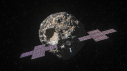
NASA has officially confirmed that its Psyche mission to an asteroid has been delayed. It was expected to launch later this year, but NASA officials confirmed on Friday that the mission wouldn’t launch this year. Continue reading “NASA’s Psyche Mission Has Been Delayed”. …more
By Shane McGlaun •
Jun. 27, 2022 at 11:30pm
Bentley has revealed another model that sits at the top of its Continental GT range. It’s called the Continental GT Mulliner, and it promises the performance and chassis enhancements found on the GT Speed. Bentley Continue reading “Bentley Continental GT Mulliner Is The New Top Of The Line”. …more
By Shane McGlaun •
Jun. 24, 2022 at 10:04pm
Every now and again, the ISS has to ignite some of its booster motors to move into a different orbit to avoid debris. This is exactly what happened late last week when the ISS had Continue reading “ISS Had To Move To Avoid Russian Debris”. …more
By Shane McGlaun •
Jun. 20, 2022 at 10:26pm
Amateur astronomers have something to look at in the night sky all month long. Five planets will be aligned in the sky for the rest of the month, visible with the naked eye, but you Continue reading “Rare Planetary Alignment Makes For A Treat”. …more
By Shane McGlaun •
Jun. 14, 2022 at 9:47pm
Porsche has announced a special very limited-edition car that will only be offered in the US called the 2023 911 Carrera GTS Cabriolet America. While Porsche is saying that it will be built in very Continue reading “Porsche 911 Carrera GTS Cabriolet America Is Only For The States”. …more
By Shane McGlaun •
Jun. 13, 2022 at 10:06pm
Astra is one of the private space companies looking to make putting satellites into orbit more affordable. However, things didn’t go as planned recently when the upper stage of an Astra rocket failed, resulting in Continue reading “Astra Rocket Fails Taking Two NASA Satellites With It”. …more
By Shane McGlaun •
Jun. 13, 2022 at 9:58pm
Cadillac plans to get seriously into racing for the 2023 season. The automaker says it plans to compete in the 2023 IMSA and WEC championships as well as returning to the 24 Hours of Le Continue reading “Cadillac Project GTP Hypercar Revealed”. …more
By Shane McGlaun •
Jun. 9, 2022 at 10:27pm
One of the critical building blocks of life, as we know it, is amino acids. Scientists in Japan have announced its spacecraft. Hayabusa2 recovered 20 different amino acids from the asteroid called Ryugu between 2018 Continue reading “Japanese Spacecraft Recovered Amino Acids From Asteroid”. …more
By Shane McGlaun •
Jun. 7, 2022 at 9:45pm
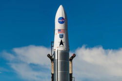
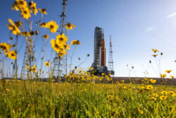
The last time the Artemis 1 rocket was on the launchpad for necessary tests before it could go into orbit, things didn’t go so well. There were three failed attempts for the wet dress rehearsal Continue reading “NASA Rolls Artemis 1 Rocket Back To Launch Pad”. …more
By Shane McGlaun •
Jun. 7, 2022 at 9:37pm
NASA has announced that it has awarded the contract to build its next-generation spacesuits for future lunar missions to two companies. The companies include Axiom Space and Collins Aerospace. Spacesuits produced by the duo will Continue reading “NASA Awards Spacesuit Contracts For Future Moon Missions”. …more
By Shane McGlaun •
Jun. 2, 2022 at 5:37pm
Last week we mentioned that a meteor shower called the Tau Herculids could produce as many as 100 meteorites per hour. However, there was a chance that none would enter the atmosphere, and the meteor Continue reading “Tau Herculids Meteor Shower Turned Out To Be Pretty Good”. …more
By Shane McGlaun •
May 31, 2022 at 8:28pm
Most of America’s looking at a long holiday weekend, and at night on May 30 and 31st, that could be something spectacular to look forward to in the night sky. There’s a possibility that a Continue reading “Crazy Meteor Shower Could Light Up The Sky”. …more
By Shane McGlaun •
May 27, 2022 at 12:14am
Giant asteroids fly past the earth frequently and rarely pose any risk to the planet. A notable asteroid will be flying by the earth this week that is the largest that will approach the earth Continue reading “A Giant Asteroid Will Pass Earth This Week”. …more
By Shane McGlaun •
May 24, 2022 at 11:58pm
For 2023, the iconic 4Runner SUV turns 40 years old. To celebrate four decades, Toyota is making 4040 2023 4Runner 40th Anniversary Special Addition SUVs available in the US. The special edition model is available Continue reading “Toyota Reveals A Special Edition 4Runner”. …more
By Shane McGlaun •
May 24, 2022 at 11:52pm
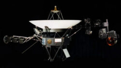
Voyager 1 is a space probe NASA launched in the 70s that is currently the farthest spacecraft from the planet. The spacecraft is 45 years old and is still sending back data. Interestingly, the spacecraft Continue reading “Voyager 1 Is Sending Back Strange Data”. …more
By Shane McGlaun •
May 20, 2022 at 9:55pm
Continue browsing more articles