NVIDIA GeForce GTX 750 Ti 2GB Video Card Review – Maxwell Architecture For Under $150
NVIDIA Maxwell Architecture
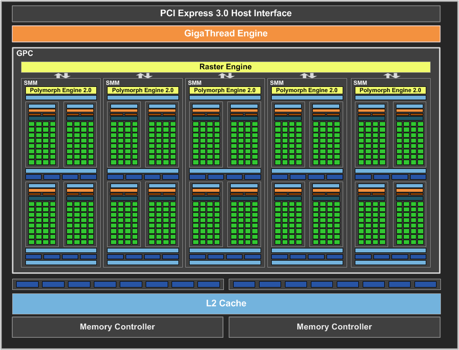
The block diagram for Maxwell looks familiar doesn’t it? The GM107 Maxwell GPU in its full implementation contains one Graphcis Processor Cluster (GPC), five Maxwell Streaming Multiprocessors (SMM), and two 64-bit memory controllers (128-bit total). This is the exact GPU that is used on the GeForce GTX 750 Ti. The GPC includes a Raster Engine and each of the five Streaming Multiprocessors (SMM) house a Polymorph Engine along with the Texture Units. The Streaming Multiprocessors are what contain the CUDA cores. ROPs are still aligned with L2 cache slices and Memory Controllers.
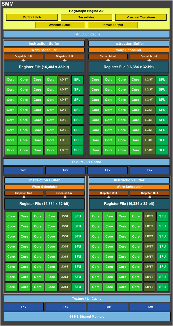
Here is a closer look at one of the Streaming Multiprocessors (SMM) and inside you can see that NVIDIA has reorganized the various blocks to make Maxwell as power efficient as possible. It should be noted that this is the first time we have seen SMM’s as they used to be called SM’s (or now what NVIDIA calls SMK’s on Kepler). Rather than a single block of 192 shaders like before, the new SMM’s are divided into four distinct blocks that each have a separate instruction buffer, warp scheduler and 32 dedicated, non-shared CUDA cores. This partitioning simplifies the design and scheduling logic, saving area and power, and reduces computation latency.