NVIDIA GeForce GeForce GTX 980 Maxwell Video Card Review
NVIDIA Maxwell GPU Architecture
Performance is a big deal for any graphics card, but NVIDIA really wanted to bring a card to market that would impress gamers with the fastest frame rates possible and also help bring 4K displays and VR technologies to the mainstream market. For many years the PC displays haven’t really changed. The majority of gamers are playing on a 1080p display and worldwide the vast majority of gamers are on sub-4K displays. NVIDIA knows that the display market is going through some rather dramatic changes right now and recognizes that the 4K display prices on monitors aimed at gamers have been quickly falling over the past year. With 4k adaptation increasing, NVIDIA knew that Maxwell would have to support 4K displays and beyond. That is why Maxwell supports HDMI 2.0 (4k resolution at 60Hz) and something called Dynamic Super Resolution (DSR) that allows you ton run a game at a higher resolution and then resizes the frames with a 13-tap Gaussian filter. This new form of ‘downsampling’ gives you the crisper visuals of a 4K panel without the need to run out and purchase a 4K display. Virtual Reality (VR) also needs higher performing GPUs as there are two displays instead of one and that is doubling the performance demands. NVIDIA had to figure out an architecture that allowed consumers to go out and buy a 4K display and triple A game title and enjoy them an an acceptable frame rate.
Performance is easy to get when you can go bigger and better, but NVIDIA was facing a market that wanted smaller PCs and better energy efficiency. The days of building PC’s with multiple-GPUs in massive full towers might very well be slowing down and in the notebook market we are all finding that notebooks are becoming thinner. NVIDIA had to find a way to get the performance they knew the market was needing, but needed to deliver it in a package that would work both desktops and laptops. That is why NVIDIA took what they learned on building the NVIDIA Tegra K1 and did some major things with with the Maxwell architecture to make everything work.
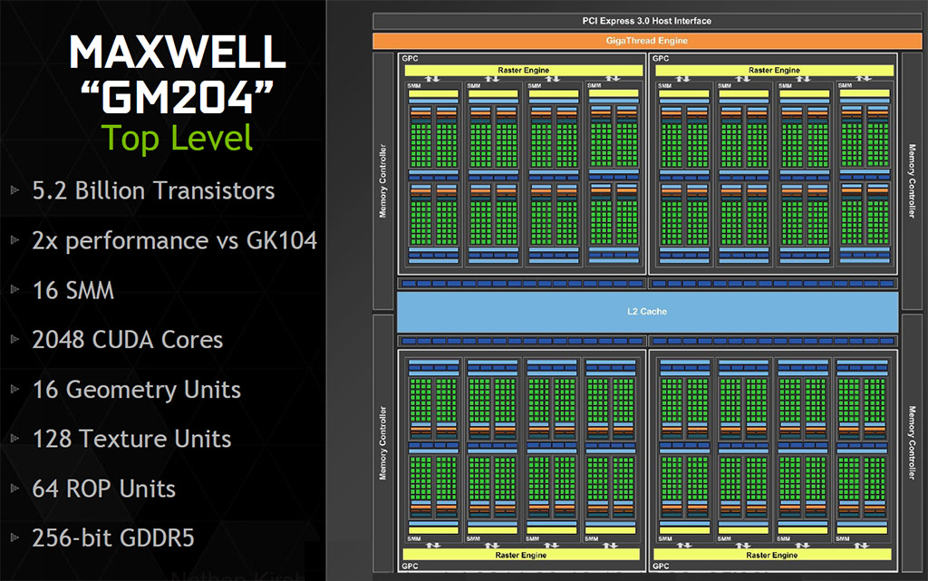
The image above is a top level overview of the GM204 block diagram. The GM204 GPU has 5.2 billion transistors and it is double the performance of the GK104 ‘Kepler’ GPU found on the GeForce GTX 680. NVIDIA has doubled up on the SMM’s, Geometry and the ROPs. The texture units were kept the same as NVIDIA felt that they were doing fine there and kept it the same. The GDDR5 memory clock speeds was increased as well as overall memory efficiency, so NVIDIA was able to go with a 256-bit bus interface on Maxwell.
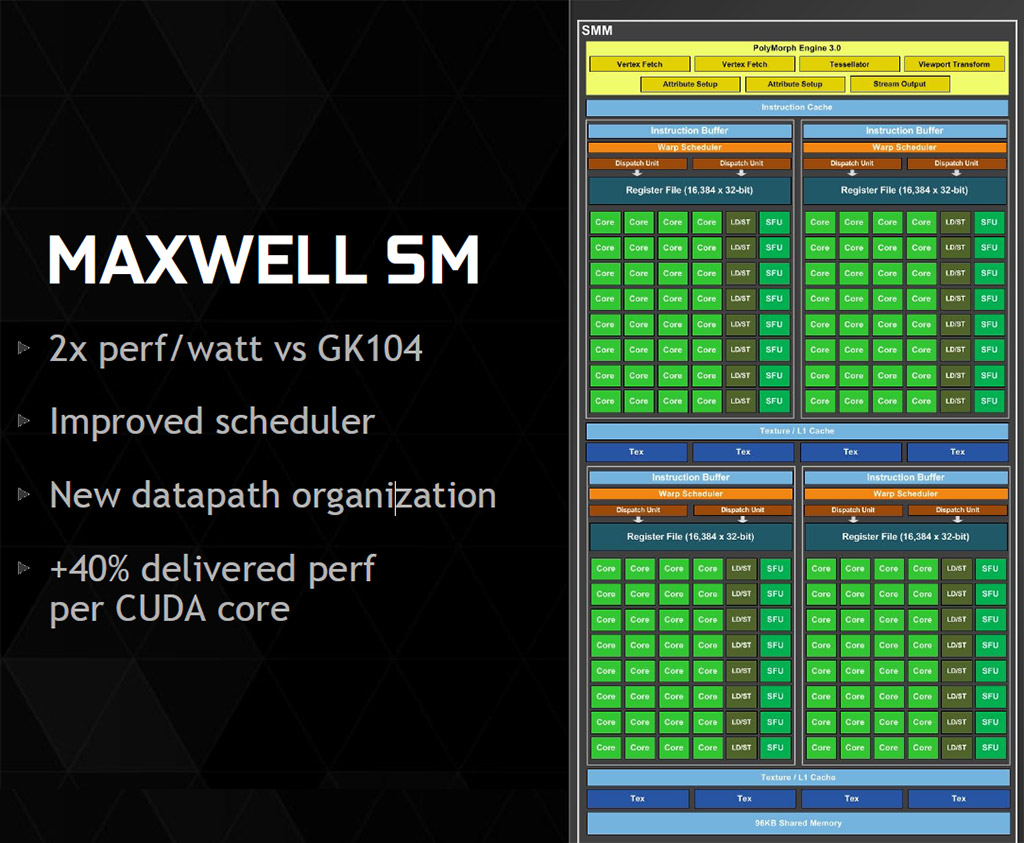
The Maxwell GM204 has a new Streaming Multiprocessor (SM) design and it uses the same basic architecture used on the first version of Maxwell, which was the GM107 GPU used on the GeForce GTX 750 and 750 Ti. NVIDIA was able to come up with a more efficient design by changing the data path organization. NVIDIA moved from a 192-CUDA core arrangement (a non-power-of-two organization) on Kepler to a 128-CUDA core arrangement per SM. This configuration aligns with warp size to save space and power versus the design on Kepler as at times NVIDIA often found all the SM units were not full and that hurt the efficiency of the GPU. By going down to 128 cores per SM and some scheduler improvements the designers at NVIDIA were able to get 40% more performance per CUDA core. NVIDIA also increased the L2 cache size from 512K in the GK104 to 2MB in GM204!
Let’s move along and take a look at the GeForce GTX 980 reference card!