AMD QuadFX FX-70 Platform Performance & Overclocking
Overclocking The QuadFX System
With the latest BIOS (0124) installed on the ASUS L1N64-SLI WS motherboard and the new 4-pin reference heat sinks with thermal pads installed on the test system we started overclocking to see how high we could get the system with no modifications at all to any of the components.
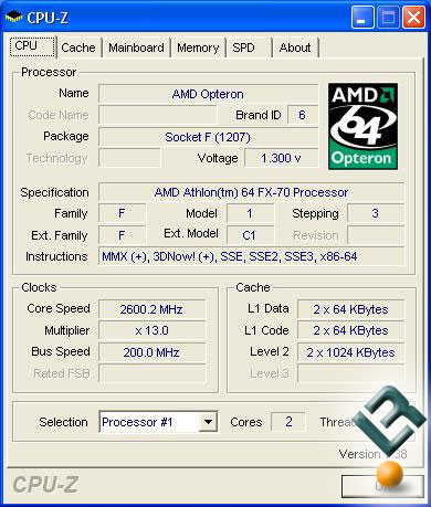
The starting point with all defaults loaded in the BIOS was 2.6GHz at 1.3V according to CPU-Z 1.38. Let’s see if we can make our FX-70 an FX-74 by adjusting the multiplier up to 15 and keeping the HyperTransport bus speed the same.
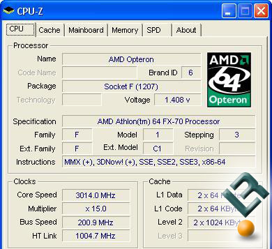
We quickly found out that using a multiplier of 14 required no changes at all, but to hit 15x we had to increase the voltage on the board to the highest setting possible in the BIOS (1.35V). In a matter of minutes we had overclocked our FX-70 to FX-74 frequencies.
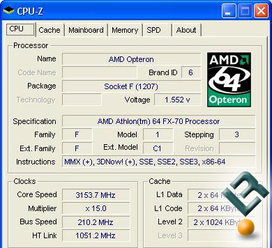
Knowing that the processor could then be overclocked higher by increased the bus speed we were able to get another 10MHz with a little more tinkering in the BIOS. Speaking of the BIOS, let’s take a look at the settings that were changed to reach this 654MHz overclock.
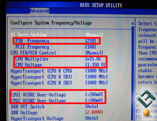
All the settings that were changed were found in the ‘advanced’ menu under the system frequency/voltage sub menu. The first thing to do is change AI Overclocking and CPU FID/VID Control from Auto to Manual. Once these have been changed to manual all the settings we need will pop up. Notice the CPU voltage needs to be changed in two spots on this board. Under CPU FID/VID Control the CPU Voltage goes up to 1.350V, which wasn’t enough to hit more than 3GHz on our test system. To reach above 200MHz on the FSB frequency we have to go down to the general voltage section and max out the CPU 1/2 VCORE Over-Voltage section. By adding 200mV to each processor we were able to reach 210MHz x 15 with some stability and 207MHz x 15 with full system stability. This is also the menu where you can mess with all the other voltages on the board. We didn’t have to change any other voltages, but since we were running 4GB of CL4 memory we bumped up the voltage on the modules to 2.0V, which is not much more the suggested memory voltage.
Interesting Fact: Many motherboard vendors frequently mis-label the main clock signal on the motherboard as the FSB when in-fact there is not front side bus. Its just the main 200MHz signal that other signals (like the CPU) are driven off of. So if you are wondering why we are talking about the FSB when AMD doesn’t have one this is why. Since the pictures show FSB we say that, since we don’t want to confuse our readers any more than they already are.
For Those That Like To Drop The Multiplier
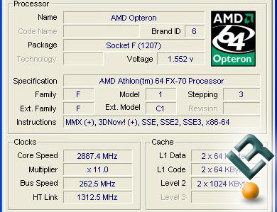
By dropping the multiplier we were able to reach 263MHz x 11, which was rock solid and got the system at 2.9GHz. When comparing the benchmark data from both overclocks it seems that the overall clock frequency matters most and the system running 207MHz x 15 meant better benchmark numbers than 263MHz x 11. Now that we which overclocking method works the best for our system let’s take a look at performance numbers.
Remember that our overclocking numbers will vary from yours as every platform is different. We used the stock heatsinks and left the thermal pads on them, so more than likely you’ll see better numbers than ours with improved cooling.
Comments are closed.