ASUS P8P67 and P8P67 Deluxe Intel Sandy Bridge Motherboard Review
ASUS P8P67 Deluxe and P8P67 Motherboard Layout
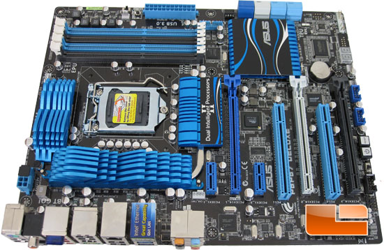
The ASUS P8P67 Deluxe motherboard is quite an attractive motherboard. It comes decked out in blue and black which will make a sharp statement if you are installing it into a windowed case.
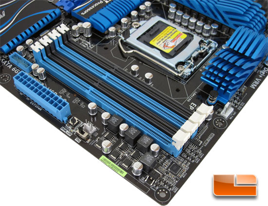
Starting out near the CPU Socket, it is worth mentioning again that the ASUS P8P67 Deluxe uses a 16+2 phase VRM design. Closer to the DIMM slots there are a few key points worth mentioning about the ASUS P8P67 Deluxe as well. Immediately to the right of the 24 pin power is the MemOK button as well as the TPU switch. To the left of the 24 pin power is the on board header for the front panel USB3. If you are installing the ASUS P8P67 into a case that doesn’t have USB3, there is no need to worry. ASUS has provided a pair of them that will install into a 3.5″ drive bay. Taking a look at the DIMM slots we see that there are four slots divided into color coded pairs. The ASUS P8P67 Deluxe will support up to 16GB of memory at speeds as fast as 2133MHz.
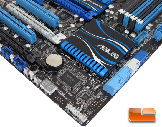
The ASUS P8P67 Deluxe has a total of eight SATA ports. Four of them support up to SATA2 while four of them will support SATA6. The two white SATA ports are SATA6 which are controlled by the Intel P67 chipset, and the two dark blue SATA ports are SATA6 controlled by the Marvell PCIe 9128 SATA6 controller. On the corner of the ASUS P8P67 Deluxe we have the pin out for the front panel which includes the power and reset switches and front panel LEDs for power and hard disk activity. Sliding up the left edge of the board we have the LED display which will display post codes, as well as a pair of 3pin fan headers. Beyond the fan headers is a pair of USB2 headers for the front panel or expansion slot bracket. Moving away from the edges of the board we have several chips that are worth mentioning. First of these is just within the corner of the ASUS P8P67 Deluxe motherboard and that is the TPU processor; this is the chip that calculates the Auto Tuning of the CPU. How well does it work? I guess we will have to test it out when we start our overclocking. Just below the left PCI slot is the PCI controller, this is an asmedia 1083 and specifics on that can be found here.
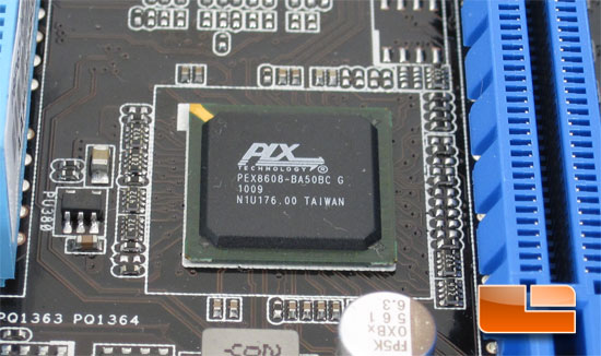
The ASUS P8P67 Deluxe takes advantage of a PLX PEX8608 chip to increase the total number of PCIe lanes. This particular PLX chip adds an additional eight lanes to the ASUS P8P67 Deluxe for a total of 24 PCIe lanes, twenty of which are usable by the graphics cards in a couple different combinations:
- 1 PCIe x16
- 2 PCIe x8/x8
- 3 PCIe x8/x8/x4
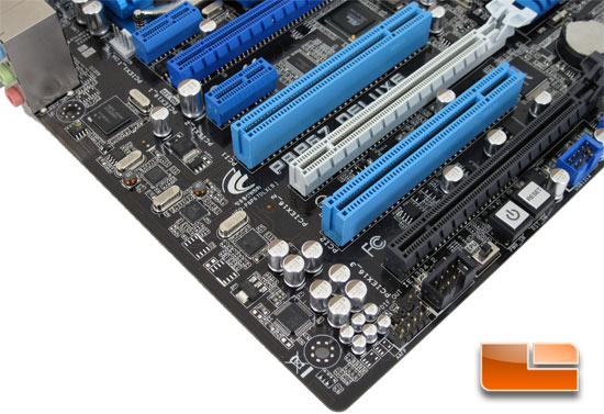
As you quite likely deduced, since we can run the PCIe configuration at x8/x8/x4, we have a total of three PCIe x16 expansion slots on the ASUS P8P67 Deluxe. We also have a pair of PCIe x1 expansion slots and a pair of PCI expansion slots that are controlled by the ASMedia 1083 chip we mentioned above. Starting just past the blue USB2 header and working our way down, we have on board power and reset buttons, EPU switch, IEEE 1394 header and the pin out for the front panel audio. Working our way up the left side of the image we have the Realtek ALC889 high definition audio codec, a VIA VT6315N IEEE1394 host controller, Realtek 8111E Gigabit LAN Controller, the Intel 82579 Gigabit LAN controller and, last but not least, the NEC USB3 controller chip for the rear I/O panel USB3.
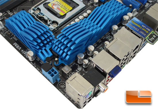
This corner doesn’t have a whole lot that is exciting to look at, but that doesn’t mean that everything here isn’t important to mention. Of course, we have the rear panel of the ASUS P8P67 Deluxe but we will take a look at that below. On the left side of the image we have the 8pin CPU power. The ASUS P8P67 takes advantage of high quality capacitors and solid chokes that surround the CPU socket.

The I/O panel of the ASUS P8P67 Deluxe doesn’t have a lot of spare room. It is packed to the hilt with 10 USB ports, two of which are super speed USB3 that offer up to ten times the performance of USB2. We also have a pair of eSATA ports and dual RJ45 LAN ports, one controlled by the Realtek 8111E and one controlled by the Intel 82579 Gigabit LAN controller. There is a single PS2 port for either a mouse or a keyboard, there is also an optical and a coaxial S/PDIF port, six audio jacks, a clear CMOS button and integrated Bluetooth.
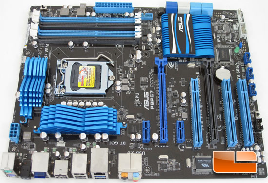
Not surprisingly, the ASUS P8P67 is remarkably similar to the ASUS P8P67 Deluxe. Instead of covering all of the same features again we are going to point out what is different between the two boards. One of the first features that is noticeably different is the cooling. The ASUS P8P67 has passive cooling, but lacks the heatpipe connecting the various heat sinks.
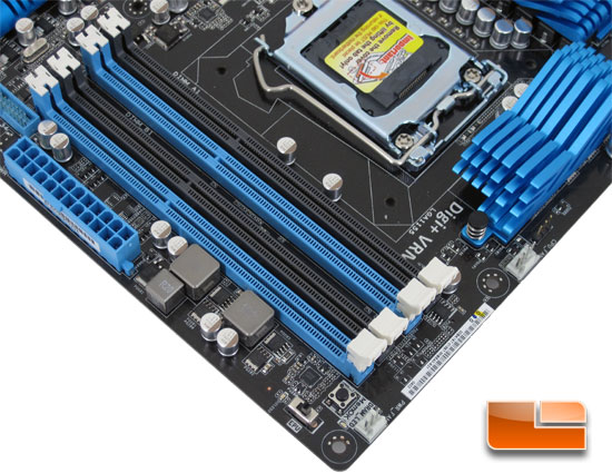
Unlike the ASUS P8P67 Deluxe that uses a 16+2 Phase VRM design the ASUS P8P67 uses a 12+2 Phase VRM design. Both boards are using the DIGI+ VRM for superior power delivery over traditional analog designs. Memory support is the same with a max of 16GB (4GBx4) and support up to 2133MHz. The MemOK! and TPU positions are slightly different though they function just the same. The above image cuts off the corner of the USB3 front panel header but it is there either way.
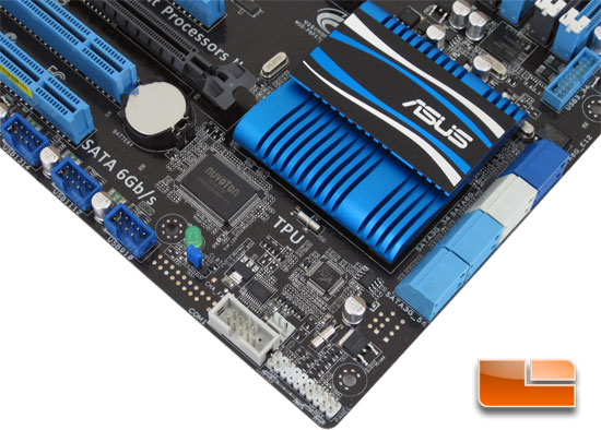
This corner of the ASUS P8P67 is nearly identical to the last. There are a few differences here to help reduce the cost of the ASUS P8P67. The layout of the SATA ports is the same, we don’t have the LED display for the post code, we are short one of the 3pin fan headers and there are three USB2 headers instead of the two that we saw on the ASUS P8P67 Deluxe. The ASMedia chip has been moved from below the PCI slot and there is no PLX chip on the ASUS P8P67 motherboard.
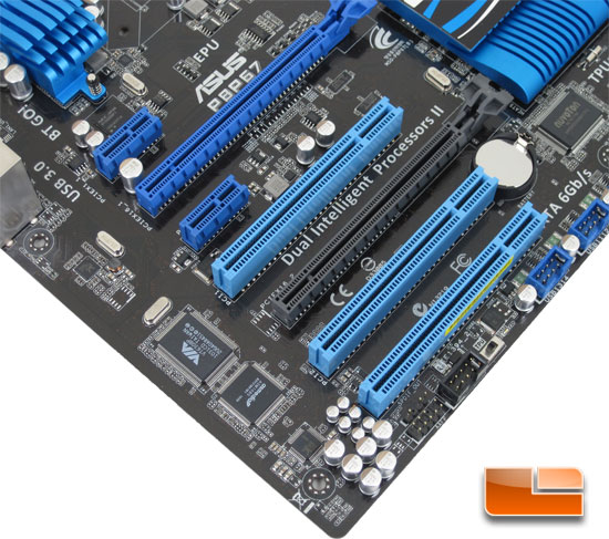
Here we can see one of the differences between the P8P67 Deluxe and the P8P67. The P8P67 only has two PCIe x16 expansion slots. The second of the PCIe x16 slots defaults to an x1 slot and must be adjusted to x4 in the BIOS to support AMD CrossfireX. Doing this does come at a cost, though, since the ASUS P8P67 doesn’t have the added PCIe lanes that the PLX chip provides on the ASUS P8P67 Deluxe. Once the second PCIe x16 slot is enabled to x4 (default x1) both PCIe x1’s and USB3 three and four (front panel USB3) will be disabled. Sliding up the left side, we have the Realtek ALC892 high definition audio codec, followed by the ASMedia 1085. Past that is the Realtek 8111E gigabit LAN controller.
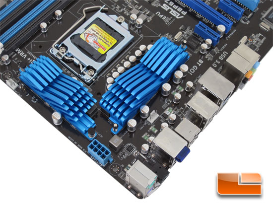
The location of the NEC USB controller chip for the I/O panel USB3 is slightly different on the ASUS P8P67 as it sits next to the first PCIe x1 expansion slot; we also have a 4pin chassis fan header here that wasn’t present on the ASUS P8P67 Deluxe.

The rear I/O panel of the ASUS P8P67 isn’t nearly as busy as the ASUS P8P67 Deluxe, but that doesn’t mean it is lacking in connectivity. There is a total of eight USB ports, two of which are USB3. There is a single RJ45 port controlled by the Realtek 8111E gigabit network controller. We have a PS2 port for both a mouse and a keyboard; there is no coaxial S/PDIF out port but we do have the optical S/PDIF out, we do not have any eSATA ports on the rear panel, but ASUS did supply an expansion bracket that has one if needed. The only other feature that is missing is the Clear CMOS button.

Comments are closed.