NVIDIA GeForce 9500 GT Video Card Preview
Under The Heat Sink
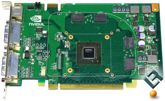
By quickly removing the four screws that hold on the GPU cooler we can see what is hiding underneath. The core is clocked at 600MHz with 32 stream processors clocked at 1.4GHz. The four memory ICs on our reference sample were part number K4J52324QE-BJ1A, which are rated at 1000MHz at 1.9V and are Lead-free and RoHS-compliant.
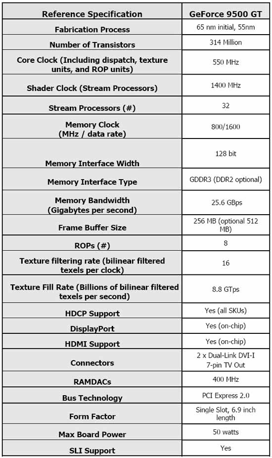
Here is the feature chart that NVIDIA provided us for the GeForce 9500 GT. The only thing we noticed that was incorrect in this chart is the memory clock frequency as it shows 800MHz and our card was running 1000MHz on the memory according to CPU-Z (see the screen shot on the next page). This also means the memory bandwidth information in the chart above is incorrect.
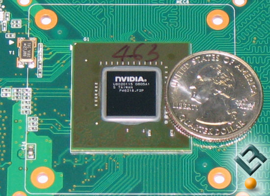
Here is a shot of the GPU core with a US quarter sitting by it to give you an idea of how big it actually is. All of the initial GeForce 9500 GT GPUs will be manufactured at 65nm with a 55nm refresh following down the road. The GPU is comprised of 314M transistors and is small considering how big the GTX280 package is.
Comments are closed.