NVIDIA GF100 Fermi Architecture and Performance Preview
GF100 Architecture In-Depth
Rather than trying to explain the GF100 Architecture ourselves we will let NVIDIA tell you about their own GPU design.
GF100 GPUs are based on a scalable array of Graphics Processing Clusters (GPCs), Streaming Multiprocessors (SMs), and memory controllers. A full GF100 implements four GPCs, sixteen SMs and six memory controllers. We expect to launch GF100 products with different configurations of GPCs, SMs, and memory controllers to address different price points. For the purpose of this whitepaper, we will focus on the full GF100 GPU.
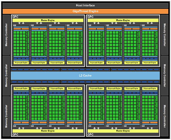
CPU commands are read by the GPU via the Host Interface. The GigaThread Engine fetches the specified data from system memory and copies them to the framebuffer. GF100 implements six 64-bit GDDR5 memory controllers (384-bit total) to facilitate high bandwidth access to the framebuffer. The GigaThread Engine then creates and dispatches thread blocks to various SMs. Individual SMs in turn schedules warps (groups of 32 threads) to CUDA cores and other execution units. The GigaThread Engine also redistributes work to the SMs when work expansion occurs in the graphics pipeline, such as after the tessellation and rasterization stages.
GF100 implements 512 CUDA cores, organized as 16 SMs of 32 cores each. Each SM is a highly parallel multiprocessor supporting up to 48 warps at any given time. Each CUDA core is a unified processor core that executes vertex, pixel, geometry, and compute kernels. A unified L2 cache architecture services load, store, and texture operations.
GF100 has 48 ROP units for pixel blending, antialiasing, and atomic memory operations. The ROP units are organized in six groups of eight. Each group is serviced by a 64-bit memory controller. The memory controller, L2 cache, and ROP group are closely coupledscaling one unit automatically scales the others.
GPC Architecture
GF100s graphics architecture is built from a number of hardware blocks called Graphics Processing Clusters (GPCs). A GPC contains a Raster Engine and up to four SMs.
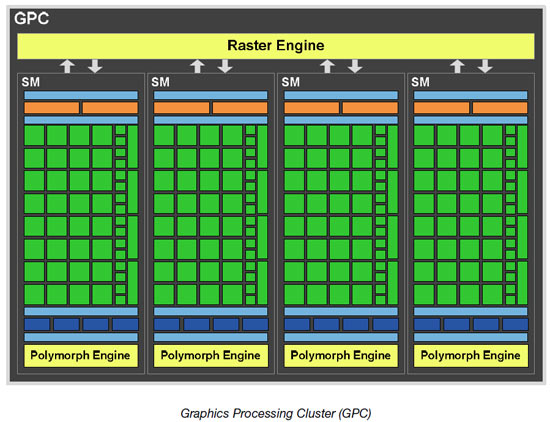
The GPC is GF100s dominant high-level hardware block. It features two key innovationsa scalableRaster Engine for triangle setup, rasterization, and z-cull, and a scalable PolyMorph Engine for vertex attribute fetch and tessellation. The Raster Engine resides in the GPC, whereas the PolyMorph Engine resides in the SM.
As its name indicates, the GPC encapsulates all key graphics processing units. It represents a balanced set of vertex, geometry, raster, texture, and pixel processing resources. With the exception of ROP functions, a GPC can be thought of as a self contained GPU, and a GF100 has four GPCs!
On prior NVIDIA GPUs, SMs and Texture Units were grouped together in hardware blocks called Texture Processing Clusters (TPCs). On GF100, each SM has four dedicated Texture Units, eliminating the need for TPCs. For simplicity, we will only refer to the SM going forward.
Parallel Geometry Processing
Previous GPU designs have used a single monolithic frontend to fetch, assemble, and rasterize triangles. This fixed pipeline provided a fixed amount of performance to an arbitrary number of parallel execution cores. As applications differ in their workload, this pipeline was often bottlenecked or underutilized. The difficulty of parallelizing rasterization while maintaining API order also discouraged major innovations in this area. While the single frontend design has worked well in past GPU designs, it became a major roadblock as the need for geometric complexity increased.
The use of tessellation fundamentally changes the GPUs graphics workload balance. With tessellation, the triangle density of a given frame can increase by multiple orders of magnitude, putting enormous strain on serial resources such as the setup and rasterization units. To sustain high tessellation performance, it is necessary to rebalance the graphics pipeline.
To facilitate high triangle rates, we designed a scalable geometry engine called the PolyMorph Engine. Each of the 16 PolyMorph engines has its own dedicated vertex fetch unit and tessellator, greatly expanding geometry performance. In conjunction we also designed four parallel Raster Engines, allowing up to four triangles to be setup per clock. Together, they enable breakthrough triangle fetch, tessellation, and rasterization performance.
The PolyMorph Engine
The PolyMorph Engine has five stages: Vertex Fetch, Tessellation, Viewport Transform, Attribute Setup, and Stream Output. Results calculated in each stage are passed to an SM. The SM executes the games shader, returning the results to the next stage in the PolyMorph Engine. After all stages are complete, the results are forwarded to the Raster Engines.

The first stage begins by fetching vertices from a global vertex buffer. Fetched vertices are sent to the SM for vertex shading and hull shading. In these two stages vertices are transformed from object space to world space, and parameters required for tessellation (such as tessellation factor) are calculated. The
tessellation factors (or LODs) are sent to the Tessellator.
In the second stage, the PolyMorph Engine reads the tessellation factors. The Tessellator dices the patch (a smooth surface defined by a mesh of control points) and outputs a mesh of vertices. The mesh is defined by patch (u,v) values, and how they are connected to form a mesh.
The new vertices are sent to the SM where the Domain Shader and Geometry Shader are executed. The
Domain Shader calculates the final position of each vertex based on input from the Hull Shader and Tessellator. At this stage, a displacement map is usually applied to add detailed features to the patch. The Geometry Shader conducts any post processing, adding and removing vertices and primitives where needed. The results are sent back to the Tessellation Engine for the final pass.
In the third stage, the PolyMorph Engine performs viewport transformation and perspective correction. Attribute setup follows, transforming post-viewport vertex attributes into plane equations for efficient shader evaluation. Finally, vertices are optionally streamed out to memory making them available for
additional processing.
On prior architectures, fixed function operations were performed with a single pipeline. On GF100, both fixed function and programmable operations are parallelized, resulting in vastly improved performance.
Raster Engine
After primitives are processed by the PolyMorph Engine, they are sent to the Raster Engines. To achieve high triangle throughput, GF100 uses four Raster Engines in parallel.

The Raster Engine is composed of three pipeline stages. In the edge setup stage, vertex positions are fetched and triangle edge equations are computed. Triangles not facing the screen are removed via back face culling. Each edge setup unit processes up to one point, line, or triangle per clock.
The Rasterizer takes the edge equations for each primitive and computes pixel coverage. If antialiasing is enabled, coverage is performed for each multisample and coverage sample. Each Rasterizer outputs eight pixels per clock for a total of 32 rasterized pixels per clock across the chip.
Pixels produced by the rasterizer are sent to the Z-cull unit. The Z-cull unit takes a pixel tile and compares the depth of pixels in the tile with existing pixels in the framebuffer. Pixel tiles that lie entirely behind framebuffer pixels are culled from the pipeline, eliminating the need for further pixel shading work.
Recap of the GPC Architecture
The GPC architecture is a significant breakthrough for the geometry pipeline. Tessellation requires new levels of triangle and rasterization performance. The PolyMorph Engine dramatically increases triangle, tessellation, and Stream Out performance. Four parallel Raster Engines provide sustained throughout in
triangle setup and rasterization. By having a dedicated tessellator for each SM, and a Raster Engine foreach GPC, GF100 delivers up to 8 the geometry performance of GT200.
Third Generation Streaming Multiprocessor
The third generation SM introduces several architectural
innovations that make it not only the most powerful SM yet built, but also the most programmable and efficient.
512 High Performance CUDA cores
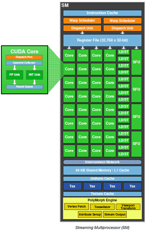
Each SM features 32 CUDA processorsa fourfold increase
over prior SM designs. GF100s CUDA cores are designed for maximum performance and efficiency across all shader workloads. By employing a scalar architecture, full performance is achieved irrespective of input vector size. Operations on the z-buffer (1D) or texture access (2D) attain full utilization of the GPU.
Each CUDA processor has a fully pipelined integer arithmetic logic unit (ALU) and floating point unit (FPU). GF100 implements the new IEEE 754-2008 floating-point standard, providing the fused multiply-add (FMA) instruction for both single and double precision arithmetic. FMA improves over a multiply-add (MAD) instruction by doing the multiplication and addition with a single final rounding step, with no loss of precision in the addition. FMA minimizes rendering errors in closely overlapping triangles.
In GF100, the newly designed integer ALU supports full 32-bit precision for all instructions, consistent with standard programming language requirements. The integer ALU is also optimized to efficiently support 64-bit and extended precision operations. Various instructions are supported, including Boolean, shift, move, compare, convert, bit-field extract, bitreverse insert, and population count.
16 Load/Store Units
Each SM has 16 load/store units, allowing source and destination addresses to be calculated for sixteen threads per clock. Supporting units load and store the data at each address to cache or DRAM.
Special Function Units (SFUs) execute transcendental instructions such as sin, cosine, reciprocal, and square root. Graphics interpolation instructions are also performed on the SFU. Each SFU executes one instruction per thread, per clock; a warp (32 threads) executes over eight clocks. The SFU pipeline is
decoupled from the dispatch unit, allowing the dispatch unit to issue to other execution units while the SFU is occupied. Complex procedural shaders especially benefit from dedicated hardware for special functions.
Dual Warp Scheduler
The SM schedules threads in groups of 32 parallel threads called warps. Each SM features two warp
schedulers and two instruction dispatch units, allowing two warps to be issued and executed concurrently. GF100s dual warp scheduler selects two warps, and issues one instruction from each warp to a group of sixteen cores, sixteen load/store units, or four SFUs. Because warps execute independently, GF100s scheduler does not need to check for dependencies from within the instruction stream. Using this elegant model of dual-issue, GF100 achieves near peak hardware performance.
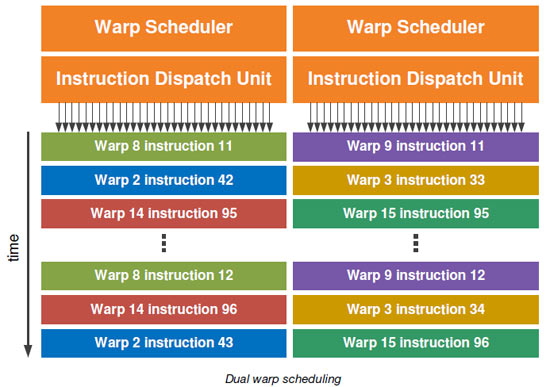
Most instructions can be dual issuedtwo integer instructions, two floating instructions, or a mix of integer, floating point, load, store, and SFU instructions can be issued concurrently. Double precision instructions do not support dual dispatch with any other instruction.
Texture Units
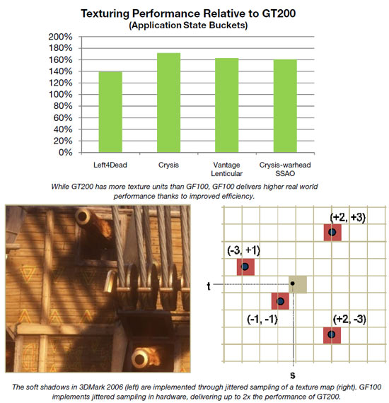
Each SM has four texture units. Each texture unit computes a texture address and fetches four texture samples per clock. Results can be returned filtered or unfiltered. Bilinear, trilinear, and anisotropic filtering modes are supported.
The goal with GF100 was to improve delivered texture performance through improved efficiency. This was achieved by moving the texture units within the SM, improving the efficiency of the texture cache, and higher clock speed.
In the previous GT200 architecture, up to three SMs shared one texture engine containing eight texture
filtering units. In the GF100 architecture, each SM has its own dedicated texture units and a dedicated texture cache. Also, the internal architecture of the texture units has been significantly enhanced. The net effect is a significant improvement in the delivered texture performance in real-world use cases such as shadow mapping and screen space ambient occlusion.
GF100s dedicated L1 texture cache has been redesigned for greater efficiency. Further, by having a unified L2 cache, the maximum available cache available for texture is three times higher than GT200, improving hit rates in texture heavy shaders.
The texture unit on previous architectures operated at the core clock of the GPU. On GF100, the texture units run at a higher clock, leading to improved texturing performance for the same number of units.;
GF100s texture units also add support for DirectX 11s BC6H and BC7 texture compression formats, reducing the memory footprint of HDR textures and render targets.
The texture units also support jittered sampling through
DirectX 11s four-offset Gather4 feature, allowing four texels to be fetched from a 128128
pixel grid with a single texture instruction. GF100 implements DirectX 11 four-offset Gather4 in hardware, greatly accelerating shadow mapping, ambient occlusion, and post
processing algorithms. With jittered sampling, games can implement smoother soft shadows or custom texture filters efficiently.
64 KB Configurable Shared Memory and L1 Cache
Shared memorya fast, programmable on-chip memory, is one of the key architectural innovations of the first generation CUDA architecture. By facilitating inter-thread communication, shared memory enabled a broad range of applications to run efficiently on the GPU. Shared memory has since been adopted by all major GPU computing standards and competing architectures.
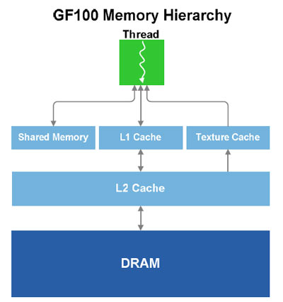
Recognizing the crucial role played by shared memory and the importance of maintaining data locality, we once again extended the GPU
memory model. GF100 incorporates a dedicated L1 cache per SM.;
The L1 cache works as a counterpart to shared memorywhile shared memory improves memory access for algorithms with well defined memory access, the L1 cache improves memory access for irregular algorithms where data addressees are not known beforehand.
On GF100 GPUs, each SM has 64 KB of on-chip memory that can be configured as 48 KB of Shared memory with 16 KB of L1 cache, or as 16 KB of Shared memory with 48 KB of L1 cache.
For graphics programs, GF100 makes use of the 16 KB L1 cache configuration. The L1 cache acts as a
buffer for register spills, allowing graceful performance scaling with register usage. For compute programs, the L1 cache and shared memory enables threads within the same thread block to cooperate, facilitates extensive reuse of on-chip data, and reduces off-chip traffic. Shared memory is a key enabler for many high-performance CUDA applications.
L2 Cache
GF100 has a 768 KB unified L2 cache that services all load, store, and texture requests. The L2 provides efficient, high speed data sharing across the GPU. Algorithms for which data addresses are not known beforehand, such as physics solvers, ray tracing, and sparse data structures especially benefit from a hardware cache. Post processing filters that require multiple SMs to read the same data require fewer trips to memory, improving bandwidth efficiency.
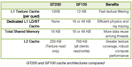
A unified cache is more efficient than separate caches. In a non-unified cache design, if one cache is oversubscribed, it cannot use the unmapped portions of other caches. Cache utilization will always be less than the theoretical peak. GF100s unified L2 cache dynamically load balances between different requests, allowing full utilization of the cache. The L2 cache replaces the L2 texture cache, ROP cache, and on-chip FIFOs on prior GPUs.
A unified cache also ensures memory access instructions arrive in program order. Where read and write paths are separate (such as a read only texture path and a write only ROP path), read after write hazards may occur. A unified read/write path ensures program correctness, and is a key feature that allows NVIDIA GPUs to support generic C/C++ programs.
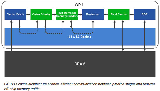
GF100 L2 cache is read/write and fully coherent compared to GT200 L2 cache which is read-only. Evicting data out of L2 is handled by a priority algorithm that includes various checks to help ensure needed data stays resident in the cache.
New ROP Units with Improved Antialiasing
GF100s ROP subsystem has been redesigned for improved throughput and efficiency. One GF100 ROP partition contains eight ROP units, a twofold improvement over prior architectures. Each ROP unit can output a 32-bit integer pixel per clock, an FP16 pixel over two clocks, or an FP32 pixel over four clocks. Atomic instruction performance is also vastly improvedatomic operations to the same address
execute up to 20 times faster than GT200, operations to contiguous memory regions execute up to 7.5 times faster.;
Performance for 8xMSAA is significantly increased on GF100 due in improvements in compression efficiency as well as additional ROP units that permit more effective rendering of smaller primitives that cannot be compressed. Increasing geometric realism in scenes increases the requirement for ROP units
to perform well when compression is not active.;
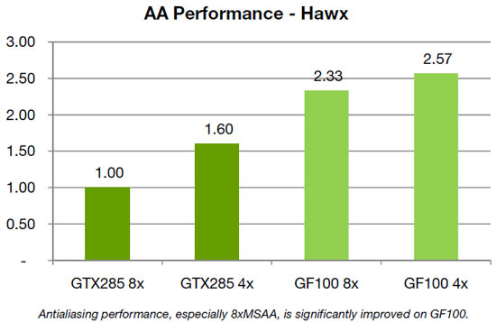
In the previous generation, performance drop in 8xMSAA modes varied significantly depending on the title; Tom Clancys HAWX is one example of a game that showed low efficiency in 8xMSAA. In GF100 the 8xAA performance is much improved. In 4xAA mode, GF100 is 1.6 faster than GT200. Comparing in 8xAA mode, GF100 is 2.3 faster than GT200, and only 9% slower than the GF100 4xAA mode.;
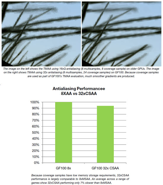
GF100 has also invested in a new 32x Coverage Sampling Antialiasing (CSAA) mode to provide the highest image quality and improve the level of perceived geometric realism in current games using alpha-to-coverage.
Current games are constrained by the limitations of API and GPU horsepower in the amount of geometry
they can render. Foliage is a particular challenge. A common technique for foliage is to create an alphatextured billboard containing many leaves, using alpha to coverage to eliminate the gaps between the leaves. The quality of the edge is determined by the number of coverage samples. In cases with only four coverage or even eight samples available, very objectionable aliasing and banding results, especially when the texture is close to the screen. With 32x CSAA, the GPU has 32 total coverage samples available, minimizing banding effects.
Transparency Multisampling (TMAA) also benefits from CSAA. TMAA benefits DirectX 9 games that are unable to use alpha-to-coverage directly because it is not exposed in the DirectX 9 API. Instead they use a technique called alpha test which produces hard edges for transparent textures. TMAA converts the old shader code in the DirectX 9 applications to use alpha-to-coverage, which combined with CSAA, produces greatly improved image quality.
Compute Architecture for Graphics
The vast improvements in per-pixel realism in recent years were made possible by programmable
shaders. Going forward, programmability will continue to be of overriding importance in allowing
developers to create next generation visual effects.
Computer graphics is a set of diverse problems with numerous approaches. Rasterization, ray tracing,
and Reyes are well recognized general rendering algorithms. Within each style of rendering, different
solutions exist for various sub-problems. Up until now, the GPU has been designed solely for
rasterization. As developers continue to search for novel ways to improve their graphics engines, the
GPU will need to excel at a diverse and growing set of graphics algorithms. Since these algorithms are
executed via general compute APIs, a robust compute architecture is fundamental to a GPUs graphical
capabilities. In essence, one can think of compute as the new programmable shader.
G80 was NVIDIAs first compute architecture. Its design reflected the desire to extend the GPUs
capabilities to solve HPC style problems. For example, one of G80s key innovations, shared memory,
was instrumental in accelerating matrix multiplication, the basis of many math and physics algorithms.
GF100s compute architecture is designed to address a wider range of algorithms and to facilitate more
pervasive use of the GPU for solving parallel problems. Many algorithms, such as ray tracing, physics,
and AI, cannot exploit shared memoryprogram memory locality is only revealed at runtime. GF100s
cache architecture was designed with these problems in mind. With up to 48 KB of L1 cache per SM
and a global L2 cache, threads that access the same memory locations at runtime automatically run
faster, irrespective of the choice of algorithm.
Another area of improvement in GF100s compute architecture for gaming is in scheduling. G80 and
GT200 executed large kernels one at a time with relatively slow context switching. Since HPC
applications employ large data sets and are insensitive to latency, this model worked relatively well. In
gaming applications, no single kernel dominates, but various small kernels (cloth, fluid, and rigid bodies
for example) are executed. On GF100, these kernels execute in parallel, enabling maximum utilization of
CUDA cores.
In games that make use of compute, context switches occur at every frame, making their performance
highly critical to responsive framerates. GF100 reduces context switch time down to about 20
microseconds, making it possible to perform fine-grained context switching between multiple kernels
per frame. For example, a game may use DirectX 11 to render the scene, switch to CUDA for selective
ray tracing, call a Direct Compute kernel for post processing, and perform fluid simulations using PhysX.
As developers make more general use of the GPU, better language and debugging support becomes
crucial. GF100 is the first GPU to offer full C++ support, the language of choice among game developers.
To ease the transition to GPU programming, weve also developed Nexusa Microsoft Visual Studio
programming environment for the GPU. Together with new hardware features that provide better
debugging support, developers will be able enjoy CPU-class application development on the GPU.

Comments are closed.