NVIDIA GeForce GTX 680 Video Card Review
Taking The GeForce GTX 680 Apart
Since supposedly no one has seen a GeForce GTX 680 production card in person, we took it apart to see the layout and to take a peak at the new GK104 GPU core. First we removed the black plastic shroud that is screwed onto a metal assembly on the front of the GeForce GTX 680 graphics card.
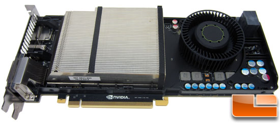
The NVIDIA GeForce GTX 680 fan shroud is held down with six screws with thread locking compound making removal a little tricky. Once you get the six screws off you can gently lift the cover off revealing the fin stack and some of the components on the PCB. This is as far as most people will ever need to go as you can easily use compressed air to blow the dust out of the custom fin stack if needed.
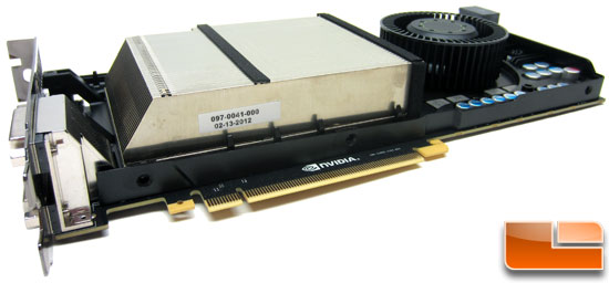
One of the first things that we noticed is that NVIDIA ended the aluminum fin stack at an angle rather than cutting them at a 90 degree angle. NVIDIA said that by providing this extra space between the heatsink and the rear bracket, hot air from the GPU is able to flow through the heatsink and exhaust out the back of the card more efficiently allowing the GPU to run cooler than with the heatsink placed flush to the bracket.
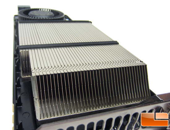
Here is another look at the end of the GPU cooler fin stack showing the fin end angle which reduces noise and improves cooling performance.
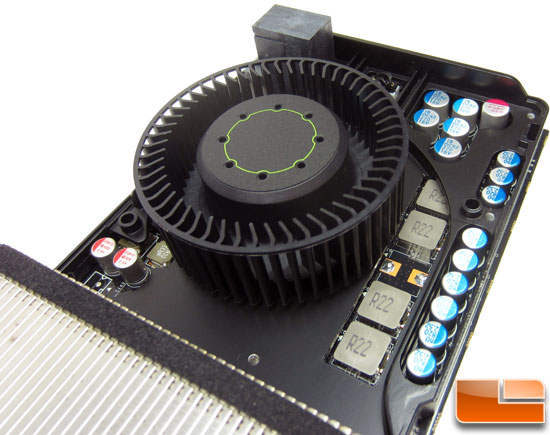
On the other end of the card you can see the power design that NVIDIA is using on the GeForce GTX680. NVIDIA went with a 4-phase power design for the GPU and a 2-phase power design for the 2GB of GDDR5 memory. Just looking at this picture you might miss some of the design changes that NVIDIA made for improved cooling. For starters they moved the main GPU power phases to the bottom edge of the card, so the cooling fan blows air across them to keep them better cooled. In order to make room for the power phases, NVIDIA move the cooling fan higher up on the card which required NVIDIA to change the orientation of the 6-pin power connectors. NVIDIA made a custom stacked connector to provide the room necessary to move the fan higher up on the PCB which also allowed a half-inch reduction in the overall PCB length. Acoustic dampening material is also used inside the GPU fan to minimize unwanted tones such as the blade passing frequency tones. NVIDIA said they are pleased with the 4+2 phase design and that it is capable of delivering plenty of power for overclocking beyond 1.2GHz on the core clock if desired. As you can tell from the image above there are some missing components on both power phases, so it looks like NVIDIA had the ability to run more phases, but didn’t need to.

Next you can remove the four larger Philips head spring screws attaching the heatsink to the video card. With the heatsink removed reveals the core for the very first time! If you ever want to change out the thermal paste this is how far you need to go. As you can see from the image above, the company that assembled this card did a great job with the thermal compound application.
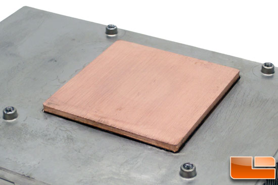
Here is a better look at the copper bottom of the GPU cooler that NVIDIA is using to make direct contact with the GK104 GPU core. NVIDIA has had some issues with getting the base machined flat in previous generations, but we are glad to report that it was fully machined and flat. Enthusiasts and overclockers will likely find lapping this copper base plate will be an easy way to improve performance as it was fairly rough and the three heatpipes are hidden safely on the other side of the plate.
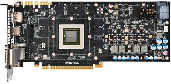
The metal bracket that covers the memory modules is held down by T7 Torx screws and our screwdriver in that size has walked off, so here is a PCB shot provided by NVIDIA.
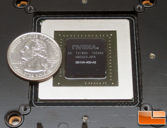
Now that the card is stripped down we can take a
good look at the heart of the GeForce GTX 680 GPU, the GK104 core shown above. The core is labeled as GK104-400-A2, which we
are guessing would be an A2 stepping of the GK104 silicon. For reference, the core is about the same size as United States quarter!

Comments are closed.