NVIDIA GeForce GTX 680 Video Card Review
Good Riddance Fermi and Hello Kepler!
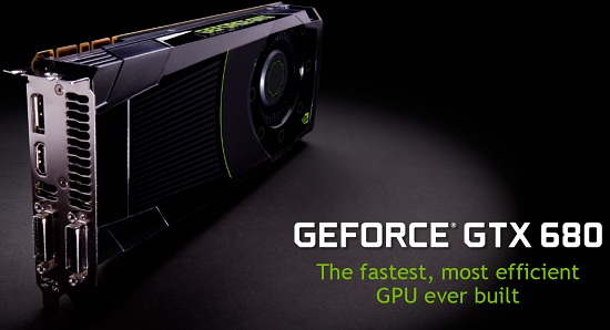
This morning NVIDIA introduced the GeForce GTX 680 video card which is the first card in the long awaited GeForce 600 series and also the first desktop GPU based on the new 28nm ‘Kepler’ core architecture. This means that the GeForce GTX 580 has been officially dethroned after over 16 months of rule! Its hard to imagine that the GeForce GTX 580 was released back in November 2010 but it was and the card has served gamers well. Priced at $499, the GeForce GTX 680 comes at the same suggested retail price as the GeForce GTX 580 did, but features a new GPU core that has 1536 CUDA Cores. The GeForce GTX 580 had just 512 CUDA cores, so with three times as many CUDA cores you know things are about to get very interesting.
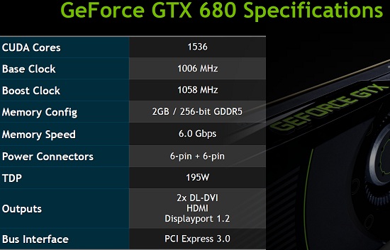
NVIDIA focused on three principles when they designed the GeForce GTX 680: Make it Faster. Smoother. Richer. By doing so they developed the Kepler architecture on an optimized 28nm process and squeezed all the performance and power enhancements out of it that they could. The GK104 is the first GPU based on this architecture and it is the core used on the GeForce GTX 680.
With a total of eight Streaming Multiprocessor (SMX) units, the GeForce GTX 680 video card has 1536 CUDA Cores. The memory subsystem of the GeForce GTX 680 consists of four 64-bit memory controllers (256-bit) with 2GB of GDDR5 memory. The base clock speed of the GeForce GTX 680 is 1006MHz and the typical Boost clock speed is 1058MHz. The typical Boost clock is based on the average GeForce GTX 680 card running a wide variety of games and applications. The actual Boost clock will vary depending on actual system conditions. GeForce GTX 680s memory speed is an impressive 6008MHz (effective). The best part of these specifications is that NVIDIA managed to get it all on a 10-inch PCB with two 6-pin PCIe power connectors and a TDP of just 195 Watts!
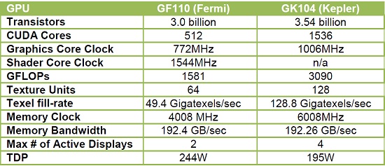
Compared to the GF110 GPU used on the GeForce GTX 580, the GK104 and the GeForce GTX 680 is a whole new beast. For starters the core clock and shader clock are now running at the same frequency. The graphics core clock is now also dynamic, but we’ll talk about that more on the next page. The transistor count is up by 18% to 3.54 Billion, but the CUDA cores have tripled and the number of texture units has doubled. The compute performance has nearly doubled from 1581 GFLOPS to 3090 GFLOPS! You would think that all this would come at the cost of increased power consumption, but that is not the case as the TDP has been lowered down to just 195Watts. NVIDIA has also doubled the number of displays that you can use off a single card, so four monitors is now supported. This is huge as you can run 3D Vision surround plus an additional monitor as an accessory display off a single card. AMD Eyefinity was a multi-monitor feature that NVIDIA couldn’t touch with a single card prior to this, so this does help build a richer gaming and overall PC experience.
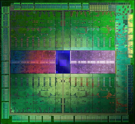
What is new with the GK104 GPU on the GeForce GTX 680? NVIDIA told us that the GK104 has roughly 3.54 Billion transistors on a die that is just 294mm. This yields a transistor density of 12 million per mm, which is competitive with what AMD has done on the Radeon HD 7000 series.
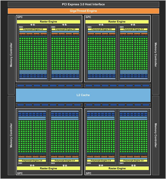
Like Fermi, Kepler GPUs are composed of different configurations of Graphics Processing Clusters (GPCs), Streaming Multiprocessors (SMs), and memory controllers. The GeForce GTX 680 GPU consists of four GPCs, eight next-generation Streaming Multiprocessors (SMX), and four memory controllers.
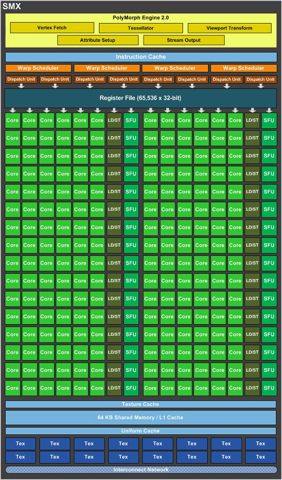
In GeForce GTX 680, each GPC has a dedicated raster engine and two SMX units. With a total of eight SMX units, the GeForce GTX 680 implementation has 1536 CUDA Cores. The CUDA cores themselves remain unchanged from the previous generation.
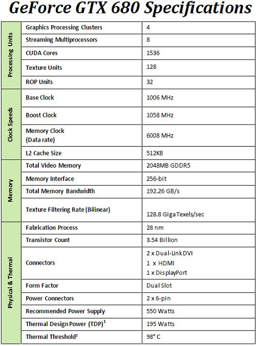
Many of our readers love specification charts and here is a good one that NVIDIA provided that shows what the GTX680 has to offer. The GeForce GTX 680s memory subsystem was completely revamped, resulting in dramatically higher memory clock speeds. Operating at 6008MHz data rate, the GeForce GTX 680 offers the highest memory clock speeds of any GPU in the industry. Tied to each memory controller are 128KB L2 cache and eight ROP units (each of the eight ROP units processes a single color sample). With four memory controllers, a full GeForce GTX 680 GPU has 512KB L2 cache and 32 ROPs (i.e., 32 color samples).
Let’s take a look at the new features this card has.

Comments are closed.