MSI P55-GD85 LGA 1156 Intel Motherboard Review
P55 GD-85 Board Images
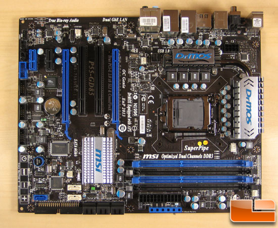
This is my first time around using a new lighting setup and I have mixed feeling about it. The most noticeable thing was how brown the PCB on this board appears under strong lighting. Coloring aside the PCB layout looks great for a P55 board. Even with 2 GPUs you still have access to a PCIe and PCI slot. All the important buttons and connectors are also either in easily accessibly locations like the edge of the board or set at 90 degree angles to facilitate ideal cable layouts.
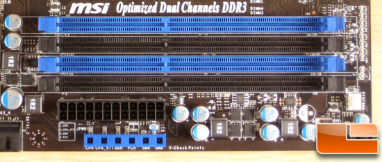
The DIMM slots support up to 16GB of DDR3 with dividers for DDR3-800, 1066, 1333, and 1600. I had no issues running my Corsair Dominator GT 2000C7 sticks at 2200C8 and beyond so the board has plenty of getup and go in that department. A nifty feature is the multimeter measurement points located below the 24-pin ATX connector.
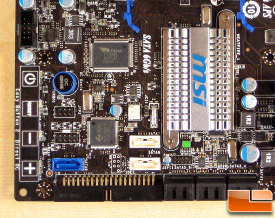
The bottom right corner of the board is packed with connectivity. Most important are the two white SATA 6 Gbps connectors provided by the Marvel SE9128 SATA 6Gbps controller. The P55 PCH provides the 6 black SATA 3 Gbps connectors while a J.Micron chip provides the lone blue SATA 3 Gbps connector and the IDE connector. The OC Genie button is a unique auto-overclocking function that we will cover later in the Overclocking section. Unique to MSI are the capacitance sensing buttons. The buttons are built into the PCB and are sensitive to your finger. I think technically they are very cool but in using them if you aren’t looking you can accidentally reset or power off your board with a glancing touch of either the power or reset button.
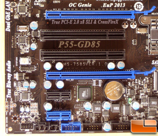
The PCIe layout gives you many options while still offering a performance configuration. In the worst-case scenario with two double-slot graphic cards you still have a PCIe x1 and PCI slot available to you. Personally, I would have removed the two PCI slots and moved the black PCIe x1 connector above the second PCIe x16 slot but rumor has it people still use PCI devices. You can see to the left of the battery a PLX PCIe switch. I’ve been looking for documentation as to what this chip’s purpose is and I’ve had no luck finding factual information. My best educated guess is that it splits some of the PCIe x1 lanes terminating at the P55 PCH rather than sucking bandwidth from the second GPU slot. This will prevent the second GPU dropping from x8 to x4 bandwidth and dropping 3D performance.
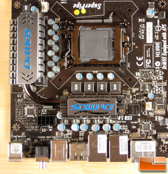
The socket itself is rather clean without a northbridge or a gigantic heatpipe rollercoaster snaking across the board. The socket is powered by an 8 + 2 PWM with a 4 phase controller with duplicated phases and a 2 phase controller for the memory controller. To the right of the heatsink you can see the NEC D720200F1 USB 3.0 controller that provides the two USB 3.0 ports on the IO panel.

The IO panel is covered in a variety of new and old connectors. To kick things off you have two PS/2 ports for keyboard/mouse, a handy clear CMOS button, audio digital/coaxial connectors, a FireWire 800 port, 6 USB 2.0 ports with a combined USB 2.0 and eSATA port, two USB 3.0 ports, two gigabit Ethernet ports, and 6 audio jacks.
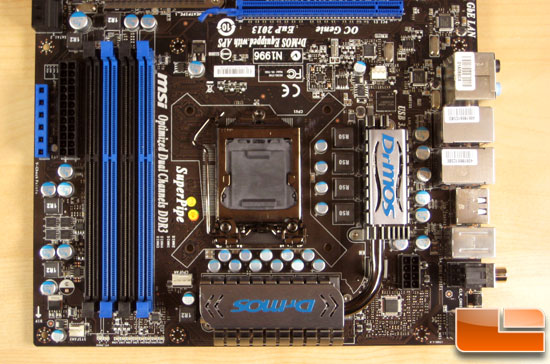
Here’s another view of the top half of the board so you can see how everything is laid out. You can barely see them, but near the bottom of the DIMM slots are a row of LEDs that indicate the number of power phases enabled on the vcore and vtt PWM.
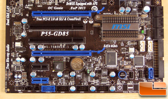
The bottom edge of the board is littered with USB 2.0 headers providing an additional 6 USB 2.0 ports and another FireWire 800 port. Either on purpose or accident the SATA 6 Gbps ports are aligned so that even with a double-slot card you won’t have a GPU heatsink covering them. The OC Genie and spare SATA 3 Gbps port are also lined up to not collide with the second GPU slot.

Comments are closed.