XFX nForce 780i SLI Motherboard Review
NVIDIA Updates The 680i SLI With a Bridge Chip!
NVIDIA has had PCI Express 2.0 compliant video cards out on the market for a month now, but didn’t offer a platform that supported this new feature. NVIDIA also didn’t have an Intel platform that could power the latest Intel 45nm Quad-Core Yorkfield processors. When it comes to selling chipsets and motherboards you have to support the latest and greatest technologies and it was obvious that NVIDIA was falling behind. NVIDIA originally claimed the 680i SLI chipset would support all 45nm dual-core and quad-core processors, but that came to an end when Intel made some changes on their latest stepping on their 45nm quad-core Yorkfield processors. It’s tough to promise support for something more than a year away and it’s obvious that NVIDIA said a little too much too soon. The 680i SLI motherboard series came out on November 8th, 2006 and has been in need of an update, so the 780i SLI chipset is a welcomed addition to the market.
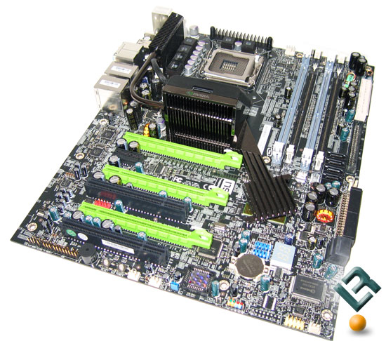
The 680i SLI and 780i SLI motherboards are undoubtedly similar, but they do have some distinct differences. The NVIDIA 780i brings the following changes:
-
Native Yorkfield and Wolfdale support
-
PCI-Express 2.0 certification
-
3-Way SLI support (3 full x16 lanes)
-
Optimized for new software including new NVIDIA Control Panel and NVIDIA System Monitor
-
Refined BIOS for overclocking (ie: ability to use half multipliers, etc.)
Basically what NVIDIA has done is some tinkering on the motherboard in order to support 45-nm quad-core processors, but that was strictly done on the board level and not in the chipset. The 680i SLI series will support 45nm dual-core processors as is, but they will not post with 45nm processors as we found out here. Since the change is on the motherboard there is nothing holding back motherboard makers from coming out with a newly revised 680i SLI motherboard to support 45nm quad-core processors. Legit Reviews recently spoke with eVGA about this and they informed us that eVGA has no plans for a new revision. This makes sense as it would hurt their 780i SLI motherboard sales.
NVIDIA has refined their BIOS for overclocking as they have added half multipliers to the mix, which allows you to better dial in your overclock. They have also some newer software revisions for NVIDIA control panel and system monitor. The new hardware features include 3-way SLI support with 3 full x16 lanes, which is great for those that have $1500+ to spend on three GeForce 8800 GTX or Ultra graphics cards. An NVIDIA nForce 200 chipset is used to help give the board it’s 3 full x16 lanes of which two are PCI Express 2.0 ready. Why are just two PCI Express 2.0 compliant?
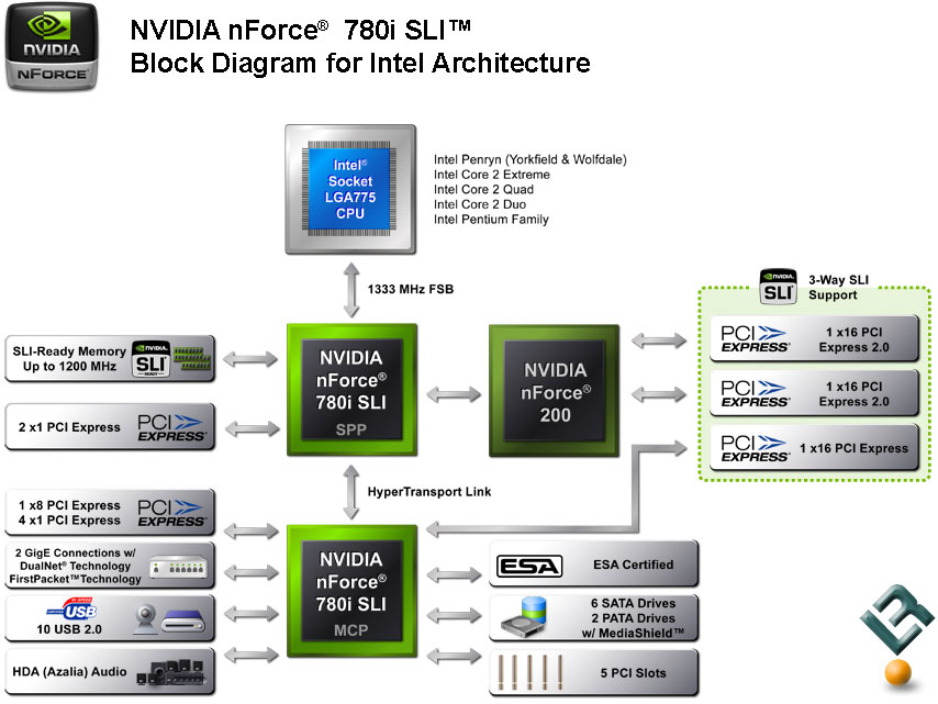
To improve the time to market for this motherboard series, NVIDIA opted to use an NVIDIA nForce 200 chipset to add the new features of the board. Traditional motherboards have two chipsets on them: a north bridge, which Nvidia calls a System Platform Processor (SPP), and the south bridge, which Nvidia calls the Media Communications Processor (MCP). The NVIDIA 780i motherboard has a third chipset on it now, which is the nForce 200. The nForce 200 connects directly to the north bridge and adds 32 lanes of PCIe 2.0 connectivity that can be split evenly between a pair of physical x16 slots. There are not enough lanes for three physical x16 PCI Express 2.0 slots, so the thrid lane goes directly through the nForce 780i SLI MCP. Of the 62 PCIe lanes, 32 are PCI Express 2.0 and they are all thanks to the nForce 200 chipset. This isn’t the best way to implement 3-way SLI support, but it works.
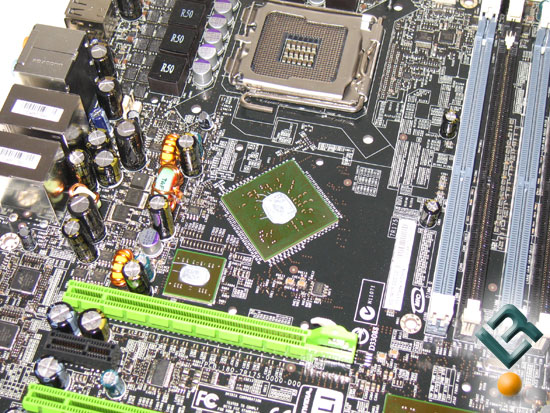
Why is it not the best way? According to PCI-SIG, the PCI Express Base 2.0 specification doubles the interconnect bit rate from 2.5 GT/s to 5 GT/s in a seamless and compatible manner. The performance boost to 5 GT/s is by far the most important feature of the PCI Express 2.0 specifications. It effectively increases the aggregate bandwidth of a 16-lane link to approximately 16 GB/s. The interface between the NVIDIA nForce 780i SLI SPP and the NVIDIA nForce 200 provides maximum bandwidth of 4.5 GT/s per link, which is below the 5 GT/s that is stated in the PCI Express 2.0 specifications. This gives the 780i SLI platform an aggregate bandwidth of a single 16-lane link to be 14.4 GB/s, which is just under what the 16 GB/s total bandwidth that a PCIe 2.0 slot should have in an ideal world. What NVIDIA has done with the 780i SLI is ‘good enough’ for today’s PCI Express 2.0 graphics cards, but what about the future? The image above shows the nForce 200 chip next to the larger north bridge or System Platform Processor (SPP).
Comments are closed.