NVIDIA GeForce GTX 280 Graphics Cards by EVGA and PNY
The GeForce GTX 200 Core
The GeForce GTX 280 is designed specifically for parallel computing, incorporating unique features like shared memory, atomic operations and double precision support. In order to do this it has 240 cores running at 1.3GHz. The GeForce GTX 280 is the most powerful floating point processor ever created for the PC and is actually the largest chip NVIDIA has designed. The GeForce GTX 280 contains roughly 1.4 Billion transistors and is built with the 65nm fabrication process. With features like this it is no wonder that NVIDIA is pushing GPU use for ‘beyond gaming’ as GPUs are so powerful and heterogeneous computing is starting to take off right now. Heterogeneous computing is the idea that to attain the highest efficiency applications should use both of the major processors in the PC, the CPU and GPU.
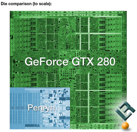
If you take the die of the Intel 45nm Penryn processor that is found in the newest quad-core processors and sit it on top of the GeForce GTX 280 you’ll get an idea of just how big this new core really is. NVIDA informed us that 80% of the transistors of a GPU are used for computation compared to just 4% for a CPU, which we thought was interesting.
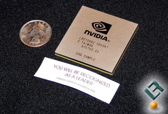
Placing the GTX 280 next to the U.S. quarter (25 cent piece) the diagram comes to life and the size of this chip is realized.

Since the GTX 200 series GPU is so large we figured we’d stop using change and it give it some paper money! It covers the President up and is just shy of being wider than a dollar.
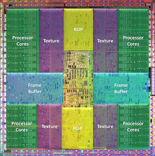
As the overlay shows, the stream processor clusters, texture units, ROPs, and frame buffer memory partitions are located in a grid layout in the GPU. NVIDIA informed us that the GTX 200 series GPU is the largest, most complex chip TSMC has ever manufactured.
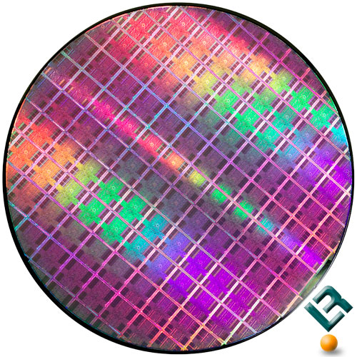
The wafer shot shows just how big the GT200 is, and also hints to to fact this this is going to be an expensive part to produce. If you count the number of full dies on that wafer, you’ll see there are only 94 or 95 complete cores and that is if all pass testing!
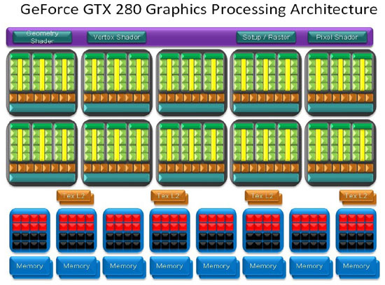
As previosuly noted, the new GeForce GTX 200 GPUs implement a second generation of unified visual computing architecture. While the foundation of both architectures is a scalar/unified/DirectX 10 processing core, GeForce GTX 200 GPUs provide many more architectural enhancements than simply a dramatic increase in the number of functional and processing units. The image above represents the GeForce 280 GTX in graphics mode. You can see the shader thread dispatch logic at the top, in addition to setup and raster units. The ten TPCs each include three SMs, and each SM has 24 processing cores for a total of 240 scalar processing cores. ROP (raster operations processors) and memory interface units are located at the bottom.
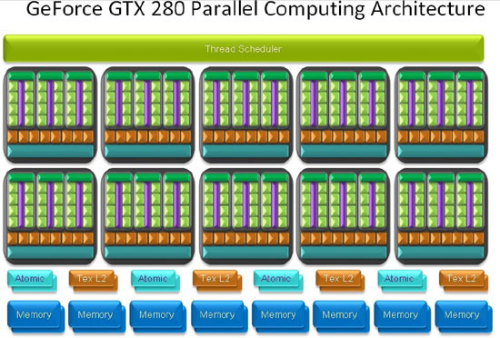
The image above shows a high-level view of the GeForce GTX 280 GPU parallel computing architecture. A hardware-based thread scheduler at the top manages scheduling threads across the TPCs. Youll also notice the compute mode includes texture caches and memory interface units. The texture caches are used to combine memory accesses for more efficient and higher bandwidth memory read/write operations. The elements indicated as atomic refer to the ability to perform atomic read-modify-write operations to memory. Atomic access provides granular access to memory locations and facilitates parallel reductions and parallel data structure management.
It should be noted that the GTX 200 series GPU cannot operate in both modes simultaneously. If you recall the G80 core used to perform ROP frame buffer blending at half speed. The new GTX 200 can perform the same tasks at full-speed. The GT200 GPU also sports twice the number of registers for longer, more complex shaders. The chip’s output buffer size has been increased by a factor of six and it offers IEEE 754R compliant double precision for improved floating-point accuracy (this is the first 64bit precision GPU). The new 512-bit memory interface and has improved z-cull and compression technology which is something critics of the GeForce 9 series wanted, so you have it now! The new core is impressive to say the least.
Let’s take a look at the EVGA and PNY cards we are reviewing today, so we can stop putting you to sleep with the technical details on the GPU.
Comments are closed.