XFX GeForce 9800 GX2 1GB GDDR3 Video Card Review
The GeForce 9800 GX2 Heat Spreader Removed
The GeForce 9800 GX2 uses a patent-pending board design for optimal acoustics, cooling, and performance. The GeForce 9800 GX2 cover can be removed by taking out a number of screws on the bottom of the card, but before we take ours apart let’s take a look at some design drawings that NVIDIA showed us.
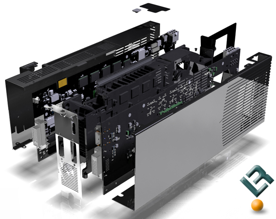
As you can see from the diagram above the NVIDIA GeForce 9800 GX2 employs a special design using two GPUs, each mounted on its own dedicated PCB. This design offers several advantages over a single PCB design:
- Each GPU dissipates heat onto its dedicated PCB. On a single-board design, both GPUs dissipate heat onto the same PCB, in effect transmitting heat to each other.
- Two PCBs allow for greater room to route traces to memory, allowing the memory modules to perform at their highest frequencies. Using this design, we managed to increase the memory clock from 900 MHz on the GeForce 8800 GT to 1000 MHz on the GeForce 9800 GX2. In contrast, the memory on the single-PCB Radeon 3870 X2 operates at 900 MHz, a 20% drop from the 1125 MHz memory on the Radeon 3870.
- A patent-pending, dual-face cooler cools both GPUs at once. This new cooler draws air from the rear and both sides of the board, cooling both GPUs before pushing the hot air out of the case. In a serial arrangement, air is only drawn from one side of the board and the hot air of one GPU is blown over the other, causing uneven cooling.
- Using two PCBs allowed us to design a graphics card with a total enclosure, enhancing the GeForce 9800 GX2s physical robustness. Aside from the PCI Express bus, there are no exposed traces, components, or open fan. This has the practical benefit of protecting the board from damage and static discharge, as well as enhancing the look and feel of the product.
The GeForce 9800 GX2 is by far the most complex multi-GPU video card that we have seen here on Legit Reviews. The ATI Radeon 3870 X2 features two GPU’s, but both are located on a single PCB like we showed you here. ATI and NVIDIA took two different approaches to how a multi-GPU card should be designed!
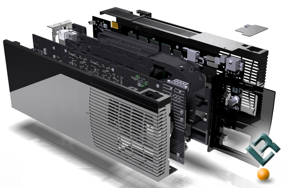
With the heat spreader removed from the XFX GeForce 9800 GX2 the fan can be seen through a cut out in the PCB. Both sides of the card are very close to being the same, so only one side will be shown in the pictures below.
The two PCB’s are actually connected by a pair of connectors at the bottom of the assembly.
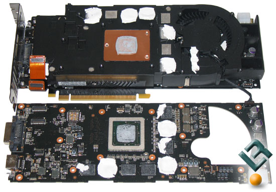
With one of the PCB’s removed we can get an idea how the heat sink works. Both cards attach to the heat stink that is located in the middle. The cooling fan then blows down the middle of the cards between the PCB’s to help cool both GPU’s at once. The GPU block was made out of copper and had plenty of thermal compound applied as you can see above. Water cooling these cards is going to be tough as the design is really going to limit the thickness of the water blocks.
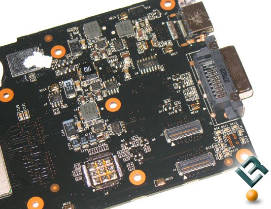
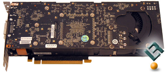
This image shows the two connectors that are used to attach the two cards together. Each card has one dual-link DVI connector onboard, which is interesting. The connection on the top right is the HDMI connector.
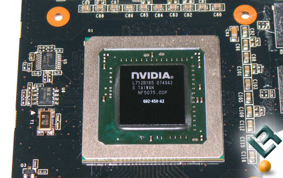
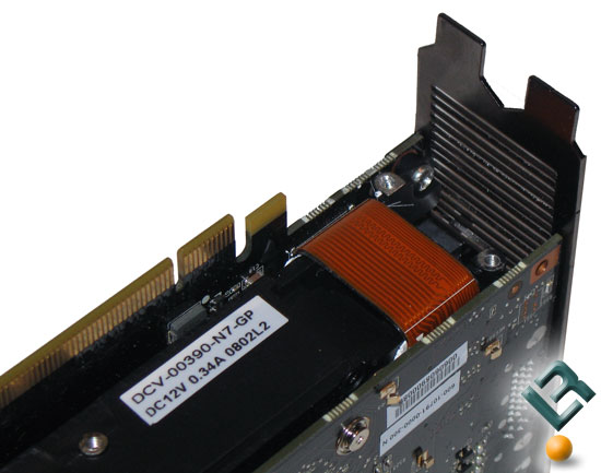
With the thermal paste cleared off the 600MHz G92 core, we can see what powers this beast. In case you don’t know the core on the GeForce 8800 GTS 512MB is labeled G92-400-A2, which is different than the core on the GeForce 8800 GT series as they are labled G92-270-A2. The GeForce 9800 GX2 that we have here is labeled G92-450-A2. The GDDR3 memory IC’s on our card were Samsung K4J52324QE-BJ1A, which are rated at 1.0ns (1000MHz).
Comments are closed.