Samsung 5nm FinFET Ready For Customers – 10 Percent More Performance
Samsung announced overnight that its 5-nanometer (nm) FinFET process technology is complete and is now ready for customers samples. Compared to 7nm, Samsungs 5nm FinFET process technology provides up to a 25 percent increase in logic area efficiency with 20 percent lower power consumption or 10 percent higher performance! Like its predecessor, 5nm uses extreme ultraviolet (EUV) lithography and that means all the 7nm intellectual property (IP) can be reused on 5nm.
In successful completion of our 5nm development, weve proven our capabilities in EUV-based nodes, said Charlie Bae, Executive Vice President of Foundry Business at Samsung Electronics. In response to customers’ surging demand for advanced process technologies to differentiate their next-generation products, we continue our commitment to accelerating the volume production of EUV-based technologies.
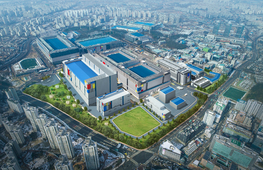
5nm production is currently taking place on the S3-line in Hwaseong, South Korea. Samsung has plans to expand its EUV capacity to a new EUV line in Hwaseong during the second half of 2019 once construction is completed. An artists rendering of how the new facility will look can be seen below. Samsung is also collaborating with customers on 6nm, a customized EUV-based process node, and has already received the product tape-out of its first 6nm chip.
This is very exciting news and we can’t wait to see the first 5nm customer wafers!