NVIDIA Tegra 650 Processor Announced – Ready To Battle x86 CPUs?
NVIDIA Tegra 650/600 – Heterogeneous Processor Architecture
Several months ago NVIDIA announced that they had developed a breakthrough APX 2500 applications processor during the Mobile World Congress in Barcelona, Spain. The APX 2500 applications processor was said to deliver an unprecedented 10 hours of 720p HD playbackan industry first for video quality and power consumption on a mobile device, as well as stunning HD camcorder and ultra-high-resolution photo imaging capabilities. Today, NVIDIA is officially announcing the Tegra 600 and Tegra 650 (CSX internal naming has been dropped). The NVIDIA Tegra 600 series processors are the second product in the Tegra line, the first being the NVIDIA Tegra APX 2500 processor, which is enabling the next generation of Windows Mobile smartphones. Tegra is the first product NVIDIA has targeted at the Mobile Internet Device (MID) and portable device space.
The NVIDIA Tegra is aimed at mobile computing devices and by just looking at the size of the chip this should be clear. The die size of the Tegra 650 and Tegra 600 is just 144mm2, which makes it ten times smaller than an Intel Atom platform that needs additional chipsets in order for it to operate. if you are wondering how much power this 144mm2 die uses you will be shocked to learn at idle it uses less than 100 mW, and when decoding a HD video stream at full power it is consuming around 2 watts total. NVIDIA expects around 25 hours of video playback and around 130 hours of audio playback!
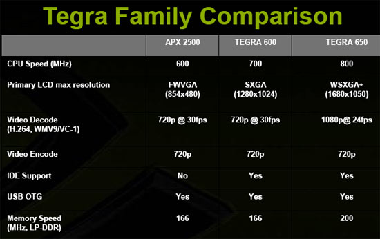
As noted in the introduction NVIDIA is launching two products based in the Tegra line. The Tegra 600 operates with a core frequency of 700MHz, while the Tegra 650 operates at 800MHz. The primary LCD resolution on the Tegra 600 is 1280×1024 (SXGA), while the Tegra 650 is 1680×1050 (WSXGA+).

Tegra is more than just a processor and NVIDIA is calling it a complete mobile computer on a chip. Tegra contains an ARM11 CPU, a GeForce GPU, an Image processor and an HD Video Processor along with everything else needed to function on a single die that It should be noted that Tegra is not X86 compatible, so it will be taking a different approach to the UMD market (Ultra Mobile Device) than the Via Nano or Intel Atom X86 processors for example
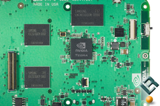
The image above is the reference PCB and it shows a Tegra processor in the center, surrounded by a couple of Samsung DRAM chips and an 8GB SAMSUNG moviNAND piece of flash memory. The Samsung moviNAND combines high-density MLC NAND flash with an MMC controller in a single chip. This reference board is what is used in the development platform seen on the next page.
Comments are closed.