Micron Ships Worlds First 176-Layer NAND Flash Memory
Micron Ships Worlds First 176-Layer NAND, Delivering A Breakthrough in Flash Memory Performance and Density
New 3D NAND boosts storage capability across mobile, automotive, client and data center applications

BOISE, Idaho, Nov. 9, 2020 Micron Technology, Inc. (Nasdaq: MU), today announced that it has begun volume shipments of the worlds first 176-layer 3D NAND flash memory, achieving unprecedented, industry-pioneering density and performance. Together, Microns new 176-layer technology and advanced architecture represent a radical breakthrough, enabling immense gains in application performance across a range of storage use cases spanning data center, intelligent edge and mobile devices.
Microns 176-layer NAND sets a new bar for the industry, with a layer count that is almost 40% higher than our nearest competitors, said Scott DeBoer, executive vice president of technology and products at Micron. Combined with Microns CMOS-under-array architecture, this technology sustains Microns industry cost leadership.
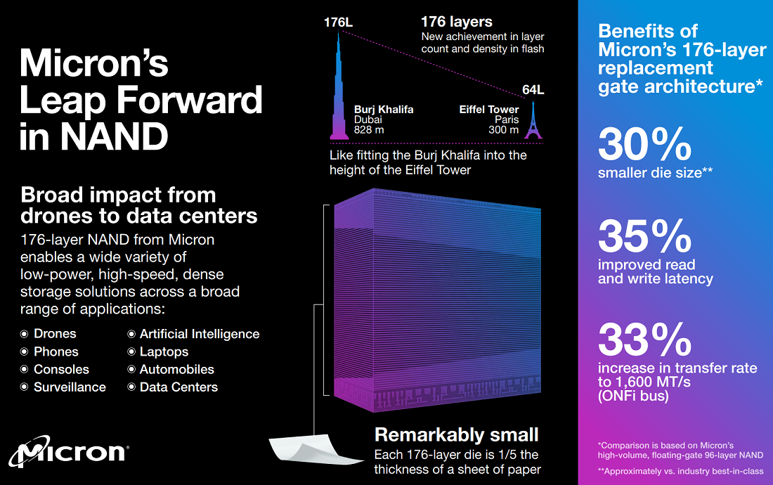
Representing Microns fifth generation of 3D NAND and second-generation replacement-gate architecture, Microns 176-layer NAND is the most technologically advanced NAND node in the market. Compared with the companys previous generation of high-volume 3D NAND, Microns 176-layer NAND improves both read latency and write latency by more than 35% dramatically accelerating application performance.1 Featuring approximately 30% smaller die size than best-in-class competitive offerings, Microns 176-layer NANDs compact design is ideal for solutions using small form factors.
Groundbreaking technology arms diverse markets with the fullest power of flash
Microns 176-layer NAND enables breakthrough product innovation for our customers, said Sumit Sadana, executive vice president and chief business officer at Micron. We are deploying this technology across our broad product portfolio to bring value everywhere NAND is used, targeting growth opportunities in 5G, AI, cloud and the intelligent edge.
With its versatile design and unrivaled density, Microns 176-layer NAND serves as an essential building block in technologists toolboxes across a broad array of sectors, including mobile storage, autonomous systems, in-vehicle infotainment, and client and data center solid-state drives (SSDs).
Microns 176-layer NAND offers improved quality of service (QoS2), a critical design criterion for data center SSDs.3 This can accelerate data-intensive environments and workloads such as data lakes, artificial intelligence (AI) engines and big data analytics. For 5G smartphones, the enhanced QoS can enable faster launching and switching across multiple apps, creating a more seamless and responsive mobile experience and enabling true multitasking and full use of 5Gs low-latency network.
Microns fifth generation of 3D NAND also features an industry-leading maximum data transfer rate at 1,600 megatransfers per second (MT/s) on the Open NAND Flash Interface (ONFI) bus, a 33% improvement.4 The increased ONFI speed leads to faster system bootup and application performance. In automotive applications, this speed will power near instant-on response times for in-vehicle systems as soon as engines are turned on, enhancing the user experience.
Micron is working with industry developers to quickly integrate the new products into solutions. To simplify firmware development, Microns 176-layer NAND offers a single-pass programming algorithm, enabling easier integration and speeding time to market.
Micron achieves unparalleled density and cost leadership with novel architecture
With the slowing of Moores Law, Microns innovation in 3D NAND is critical to ensuring that the industry can keep pace with growing data requirements. To achieve this milestone, Micron has uniquely combined its stacked replacement-gate architecture, novel charge-trap and CMOSunder-array (CuA)5 techniques. Microns team of 3D NAND experts achieved rapid advancements with the companys proprietary CuA technique, which constructs the multilayered stack over the chips logic packing more memory into a tighter space and substantially shrinking the 176-layer NANDs die size, yielding more gigabytes per wafer.
In tandem, Micron has improved scalability and performance for future NAND generations by transitioning its NAND cell technology from legacy floating gate to charge-trap. This charge-trap technology is combined with Microns replacement-gate architecture, which uses highly conductive metal wordlines6 instead of a silicon layer to achieve unparalleled 3D NAND performance. Microns adoption of this technology will also enable the company to drive aggressive, industry-leading cost reductions.
Applying these advanced techniques, Micron has increased endurance, which is particularly beneficial in write-intensive use cases from black boxes in aerospace to video surveillance recording. In mobile storage, 176-layer NANDs replacement-gate architecture results in 15% faster mixed workload performance7 to power ultra-fast edge computing, enhanced AI inference, and graphic-rich, real-time multiplayer gaming.
Availability
Microns 176-layer triple-level cell 3D NAND is in volume production in Microns Singapore fab and now shipping to customers, including through its Crucial consumer SSD product lines. The company will introduce additional new products based on this technology during calendar 2021.About Micron Technology, Inc.
We are an industry leader in innovative memory and storage solutions. Through our global brands Micron and Crucial our broad portfolio of high-performance memory and storage technologies, including DRAM, NAND, 3D XPoint memory and NOR, is transforming how the world uses information to enrich life for all. Backed by more than 40 years of technology leadership, our memory and storage solutions enable disruptive trends, including artificial intelligence, 5G, machine learning and autonomous vehicles, in key market segments like mobile, data center, client, consumer, industrial, graphics, automotive, and networking. Our common stock is traded on the Nasdaq under the MU symbol. To learn more about Micron Technology, Inc., visit micron.com.1 Comparison is based on Microns high-volume, floating-gate 96-layer NAND. When comparing with 128-layer replacement-gate NAND, read latency and write latency for Microns 176-layer NAND both improveby over 25%.
2 Quality of service (QoS) refers to the consistency and predictability of SSD response times.
3 Improved QoS is driven by a reduction in block size and less variance in read latency, as compared to Microns high-volume, floating-gate 96-layer NAND.
4 Improvement is over Microns prior two generations of 3D NAND (96-layer NAND and 128-layer NAND) which featured a maximum of 1,200 MT/s data transfer rates.
5 CMOS stands for complementary metal oxide semiconductor.
6 Wordlines are connecting wires to the gate of each NAND memory storage element in a NAND memory array. Wordlines are used to select, program and erase groups of memory cells in an array of NAND memory.
7 This is compared to Microns previous generation universal flash storage 3.1-based multichip package using floating-gate 96-layer NAND.