Intel HD Graphics 530 Has 24 Execution Units – Intel gen9 Graphics Architecture Detailed
The Intel 6th Generation Core i7-6700K and Core i5-6600K ‘Skylake’ processors feature Intel HD Graphics 530, but when the processors were released little was said about the Intel HD 530 Graphics. We knew that Intel HD 530 Graphics was the based on Intel processor graphics gen9 architecture, but other than being told that the graphics product naming conventions changed with gen9, from 4 digits to 3 we were left in the dark as to what Intel actually did on Skylake to improve graphics performance. All that changed overnight when a whitepaper titled ‘The Compute Architecture of Intel Processor Graphics Gen9‘ was published by Stephen Junkins just hours ahead of the Intel Developer Forum (IDF) that takes place in San Francisco this week.
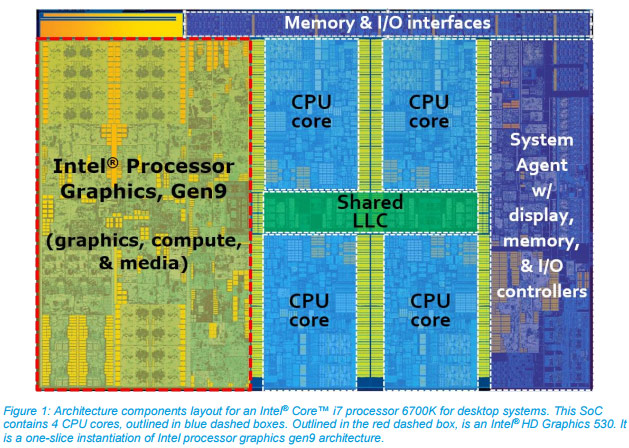
His whitepaper covers how Intel used the new gen9 architecture for the Intel HD Graphics 530 in the recently released Intel Core i7 processor 6700K for desktop form factors and other upcoming processors that will be released in the near future. The figure above offers a very high level look at the Intel 6th generation Core i7-6700K processor. You can see that Intel is using a single shared silicon die for their SoC that features multiple CPU cores, Intel processor graphics, and potentially other fixed functions all on a single shared silicon die. The architecture implements multiple unique clock domains, which have been partitioned as a perCPU core clock domain, a processor graphics clock domain, and a ring interconnect clock domain.
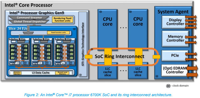
The on-die bus used on Skylake between CPU cores, caches, and Intel processor graphics is a ring based topology with dedicated local interfaces for each connected agent. This SoC ring interconnect is a bi-directional ring that has a 32-byte wide data bus, with separate lines for request, snoop, and acknowledge. Every on-die CPU core is regarded as a unique agent. Similarly, Intel processor graphics is treated as a unique agent on the interconnect ring. A system agent is also connected to the ring, which bundles the DRAM memory management unit, display controller, and other off chip I/O controllers such as PCI Express . Importantly, all off-chip system memory transactions to/from CPU cores and to/from Intel processor graphics are facilitated by this interconnect, through the system agent, and the unified DRAM memory controller. Note that Skylake has an optional eDRAM controller and supports 64-128 MB or eDRAM on its own clock domain.
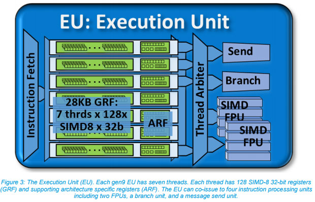
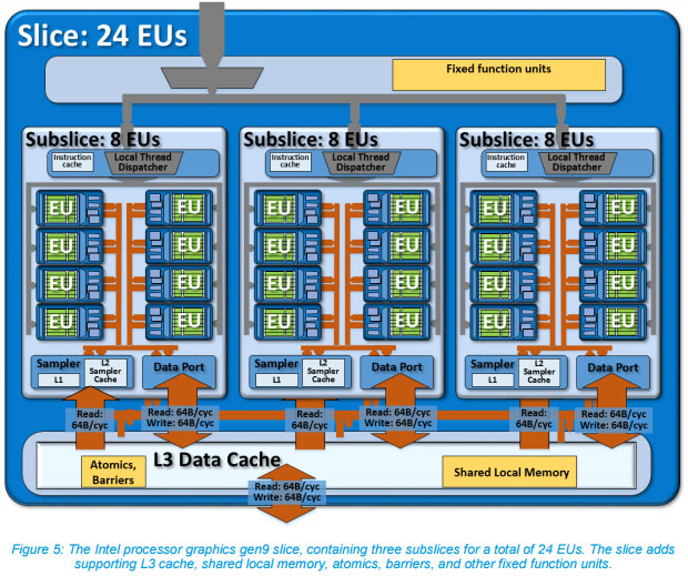
The Intel Graphics gen9 compute architecture features arrays of Execution Units (EUs) that are grouped together in clusters called a subslice. Intel designed it this way with scalability in mind as it allows them to choose the number of EUs per subslice. For most gen9-based products, each subslice contains 8 EUs. Each EU is capable of 7 threads each, so a single subslice of 8 EU’s has dedicated hardware resources and register files for a total of 56 simultaneous threads.
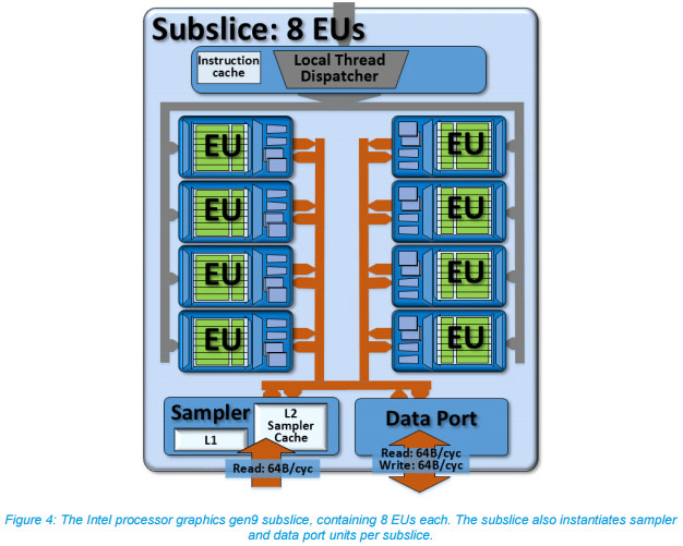
Each subslice contains its own local thread dispatcher unit and its own supporting instruction caches. The Intel Core i7 processor 6700K with Intel HD Graphics 530 has a single slice with three subslices, for a total of 24 EUs. That means it has 168 Hardware Threads!
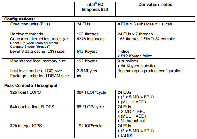
Here are some of the other Intel HD Graphics 530 performance numbers released by Intel in the white paper:
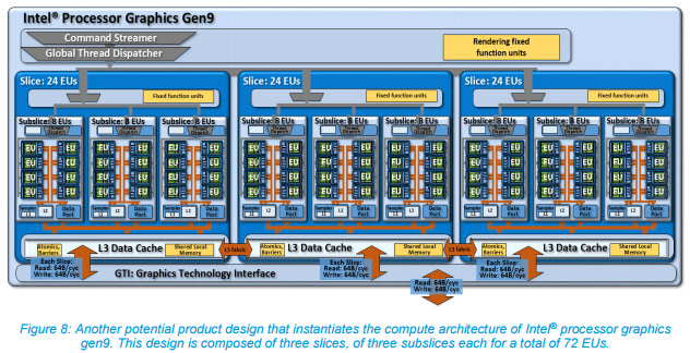
Intel also showed an image of a potential product design that is composed of three slices, of three subslices each for a total of 72 EUs!
We’ll close for now with the key changes for Intel Processor Graphics Gen9! Be sure to take a closer look at the whitepaper for all the details in much greater detail than this!
NEW CHANGES FOR INTEL PROCESSOR GRAPHICS GEN9
Intel processor graphics gen9 includes many refinements throughout the micro architecture and supporting software, over Intel processor graphics gen8. Generally, these changes are across the domains of memory hierarchy, compute capability, and product configuration. They are briefly summarized here, with more detail integrated throughput the paper.
Gen9 Memory Hierarchy Refinements:
- Coherent SVM write performance is significantly improved via new LLC cache management policies.
- The available L3 cache capacity has been increased to 768 Kbytes per slice (512 Kbytes for application data).
- The sizes of both L3 and LLC request queues have been increased. This improves latency hiding to achieve better effective bandwidth against the architecture peak theoretical.
- In Gen9 EDRAM now acts as a memory-side cache between LLC and DRAM. Also, the EDRAM memory controller has moved into the system agent, adjacent to the display controller, to support power efficient and low latency display refresh.
- Texture samplers now natively support an NV12 YUV format for improved surface sharing between compute APIs and media fixed function units.
Gen9 Compute Capability Refinements:
- Preemption of compute applications is now supported at a thread level, meaning that compute threads can be preempted (and later resumed) midway through their execution.
- Round robin scheduling of threads within an execution unit.
- Gen9 adds new native support for the 32-bit float atomics operations of min, max, and compare/exchange. Also the performance of all 32-bit atomics is improved for kernel scenarios that issued multiple atomics back to back.
- 16-bit floating point capability is improved with native support for denormals and gradual underflow.
Gen9 Product Configuration Flexibility:
- Gen9 has been designed to enable products with 1, 2 or 3 slices.
- Gen9 adds new power gating and clock domains for more efficient dynamic power management. This can particularly improve low power media playback modes