Intel Broadwell Architecture Preview – Intel Core M and Broadwell-Y
Intel 14nm Technology Details – Transistor Fins, Interconnects and More
For months we read stories online about how Intel was having a tough time ramping up production of their true 14nm technology. The good news is that Intel’s 14nm technology is qualified and in volume production and has been for some period of time. With Intel releasing Broadwell before the holidays this shouldn’t come to a shock to anyone that Intel has dialed down the 14nm process with 2nd generation Tri-gate (FinFET) transistors. When Intel unveiled the 22nm processors, they started using the first generation of the Tri-gate transistors. While the first generation was found to be good, there is always room for improvement. The upcoming 14nm Broadwell processors bring with them the 2nd generation of Tri-gate (FinFET) transistors.
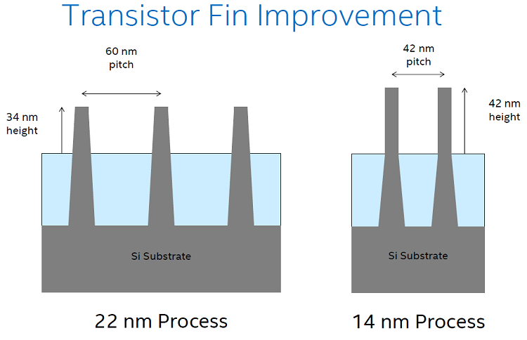
The slide above shows a drawing of a 14nm Broadwell transistor fin next to the 22nm Haswell transistor fin. Intel changed the fin profile in this generation of FinFET transistors after discovering taller and thinner had many added benefits. The fin pitch metric has gone from 60nm to a 42nm pitch, which is .70x scale factor, which is inline with the Moore’s Law. This is critical as it allows for more fins per unit length. The key reasons for this was to be able to increase drive current and overall better performance coming out of each fin. That in turn allowed Intel to depopulate fins since each fin is capable of delivering more transistor strength and that also reduced capacitance, which is key for improving power savings. The Transistor gate pitch went from 90mm to 70mm, a .78x scale factor and then interconnect pitch (very important for overall chip scaling) went from 80mm to 52mm a .65x scale factor. Intel believes they have developed a true 14nm technology with good dimensional scaling.
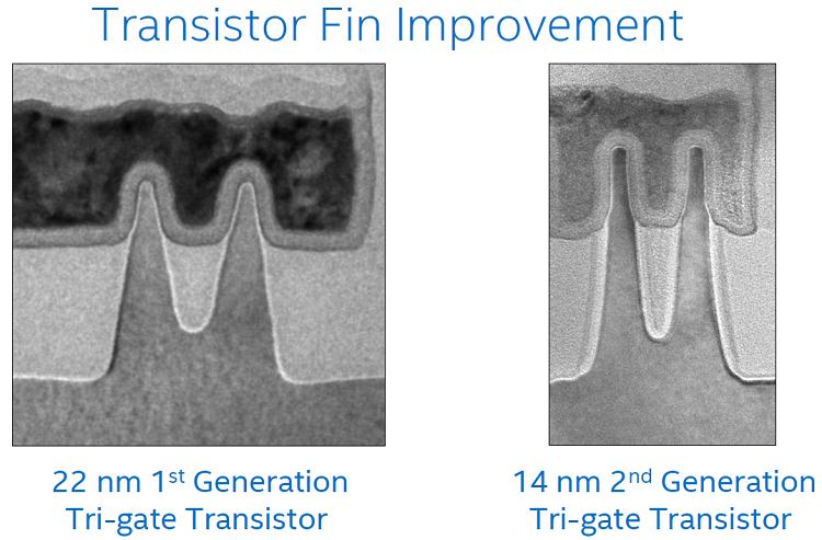
The image above is a cross section perpendicular to the fins (through the gate dielectric) from a electron micrograph. You can see the 14nm fin profiles are narrower and taller. The metal gate is sitting on top of the transistor. To summarize, the taller and thinner fins allow for increased drive current and performance. Intel was also able to reduce the number of fins allowing for improved density and lower capacitance.
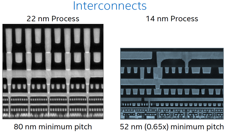
When it comes to interconnects the cross section above shows that Intel has gone from an 80nm minimum pitch to a 52nm minimum pitch. This 0.65x scaling is said to be better-than-normal interconnect scaling. SRAM Memory Cells have 0.54x area scaling from 22nm to 14nm, so the 14nm design process with 2nd generation Tri-gate transistors has lead to industry-leading densities that will likely take other companies years to match.
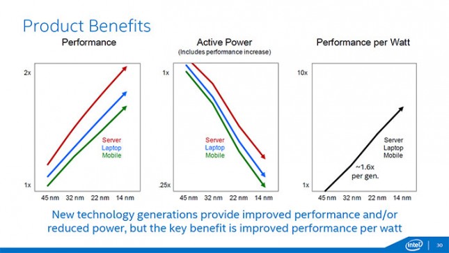
As technology advances, there is no doubt that we are going to see performance gains. That is pretty much par for the course when new processors are released by Intel. The trick is to balance the performance gains while maintaining low power usage. By taking advantage of the newest technologies available, Intel is able to increase the performance and lower the active power. When you look at performance per watt it continues to go up in this technology generation at the rate of 1.6x per generation.
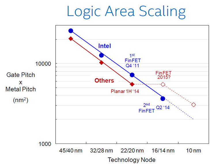
The slide above shows gate pitch times metal pitch and shows a valid metric that should areas scaling over various generations. As you can see on the 14nm node Intel has been keeping on a fairly steady ~0.53x per generation reduction when it comes to logic areas scaling and this helps show that Moore’s law is still alive and well. The other companies have had a lead in density, but they released them later in time. Intel believes that will be changing on the 16nm/14nm nodes as other companies will have to pause to develop FinFETS. Intel thinks it will they will soon be the leader when it comes to logic area scaling on both the node level and with respect to calendar time due to the other companies having to stop and figure it out. Intel will be shipping their 2nd generation FinFET before the others ship their first. Intel clearly stated that they have 14nm in volume production and they next think they are working on is 10nm.
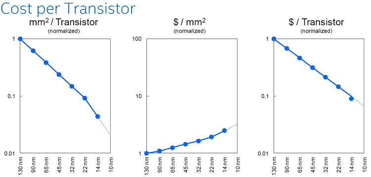
Intel has achieved better than expected area scaling due to the use of advanced double patterning techniques. The ratio has been a fairly steady line over the past six generations, but Intel is seeing better than normal scaling with the move to 14nm. This is critical as you want to use less area per transistor. When it comes to labor cost they are found to be rising due to the number of added masking steps. At the end of the day when you look at the cost per transistor it appears that Intel is continuing to scale down and this generation is actually slightly better than normal trend-line.
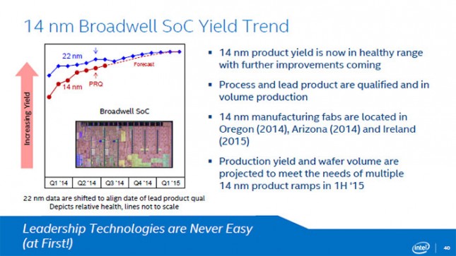
Although the 14nm technology being used for the Broadwell SoC parts is quite new, the yields are doing well. Intel has stated that the 14nm product yield is in a ‘healthy range’ with more improvements coming down the pipe. Intel currently has two fabs that are capable of the 14 nm manufacturing process one is located in Oregon while the other is located in Arizona. There is also a third fab in the works in Ireland that will be able to produce the 14 nm wafers, the Ireland fab should be golden some point in 2015.