Gigabyte GA-X99-SOC Force LN2 Motherboard With Special LGA2011-v3 CPU Socket Seen

Last night GIGABYTE had a fairly large Intel Developer Form (IDF) X99 motherboard overclocking and media gathering event that Legit Reviews was able to attend. The event had many big name overclockers at it that were given a fairly large amount of LN2, three boxes of Intel Core i7-5960X processors and all the Gigabyte X99 motherboard models they needed and they were told to have fun. There was no big cash prize or trophy to be won at the end of the night as this event was for fun and it gave a chance guys like Hi Cookie, Fugger and others to hang out and see what Haswell-E could do on Gigabyte X99 boards. Gigabyte was also hopeful that an overclocking record or two would be broken during the event, but that wasn’t the main point according to them.
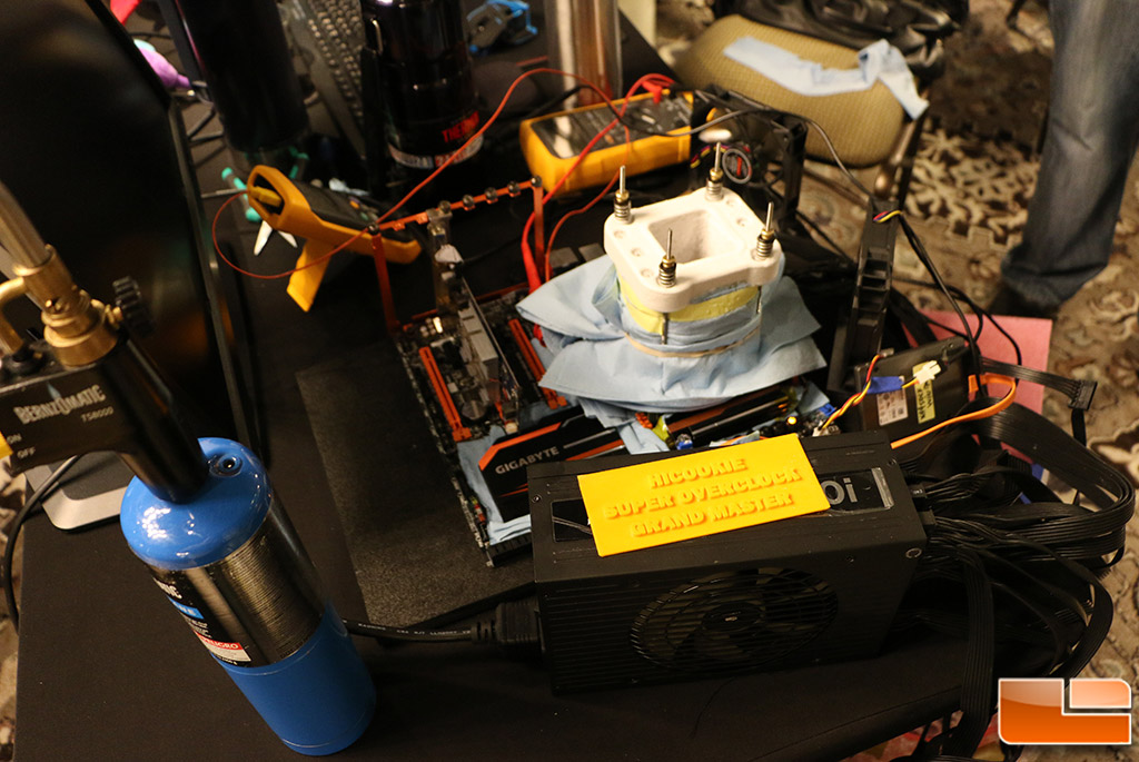


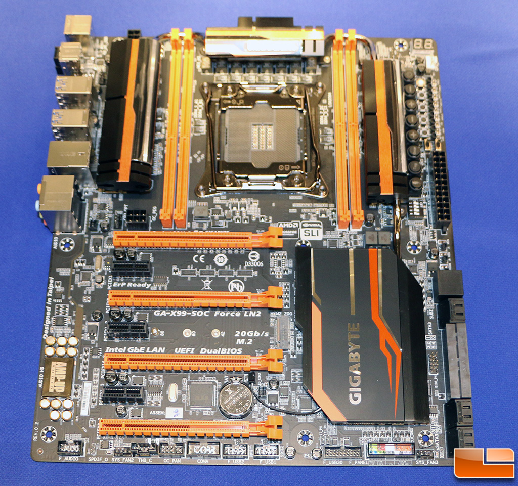
When we were at the event we spotted that Hicookie was using the Gigabyte GA-X99-SOC Force LN2 motherboard, which hasn’t been announced just yet! Gigabyte has already released the Z97-SOC FORCE LN2 motherboard for socket LGA1150 processors, but this is a new board using the Intel X99 Express chipset that has been engineered specifically for the most hardcore overclockers that need a board that can handle LN2. Gigabyte has been trying to establish the brand as having the best overclocking boards on the market and they see this board being the one to beat.
We don’t know that much about the board, but we know that it is in production and slated to arrive sometime in October if things go as planned. Gigabyte didn’t have a specifications sheet, pricing or an exact launch date, so we basically just have a bunch of pictures to show you of the board.
Nothing important to note on the back of the board.
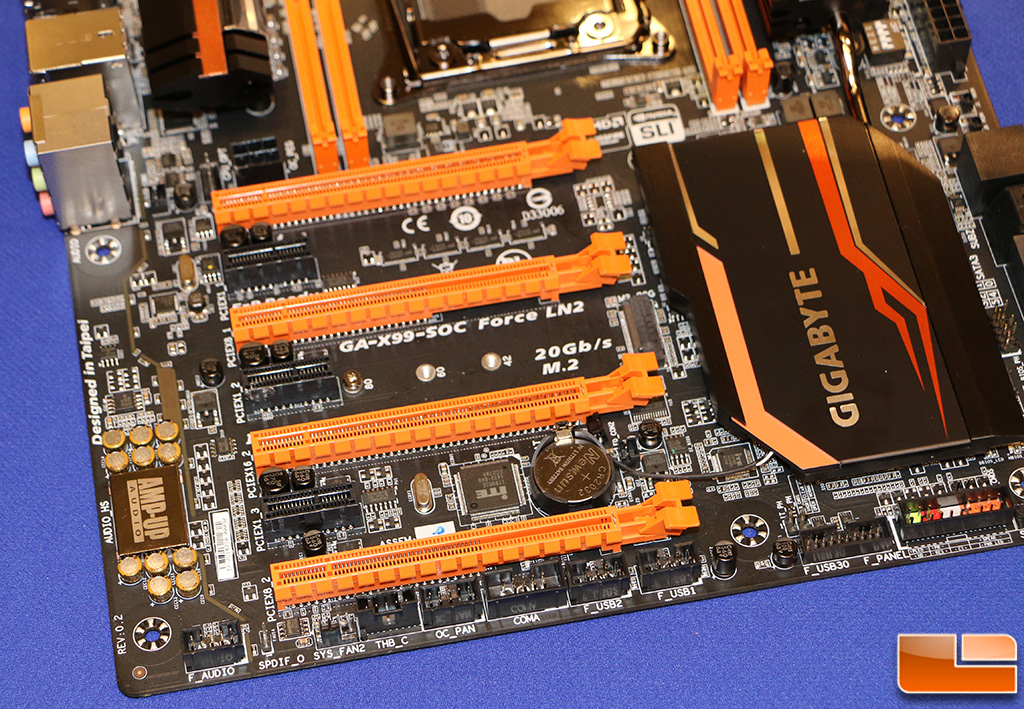
Gigabyte went with four PCI Express x16 slots and three PCI Express x1 slots on the X99-SOC Force.
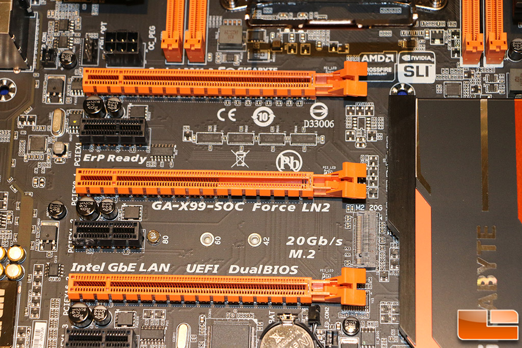
The Gigabyte Z97X-SOC Force LN2 didn’t have an M.2 PCIe slot, but it appears that the X99-SOC Force LN2 has an M.2 slot that is rated at 20Gb/s.
Gigabyte OC Touch is present and you’ll find buttons for a range of hardware overclocking functions placed directly on the motherboard, making overclocking on the fly extremely fast and easy. The OC ignition button is still there on the far left, but there is only one set of dip switches, so we aren’t sure if they are for the PCIe slots or the quad-channel memory slots. On the Z97 version these are used to manually turn on or off each channel of installed memory DIMMs or the PCIe x16 slots on the board.
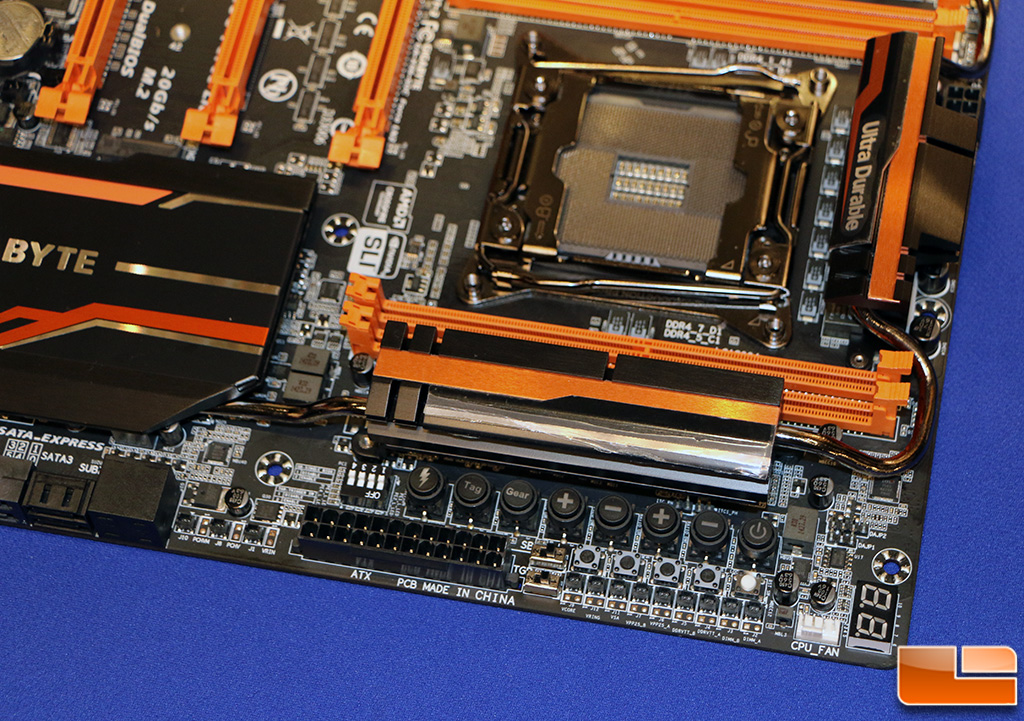
Gigabyte said that they have improved the components that feed power to Intel Haswell-E processors and went with an 8-Phase VRM powered by an 8-Pin plus 4-Pin connector configuration in addition to the traditional 24-pin ATX power connector and the optional 6-pin PCIe video card connector for additional PCIe slot power.
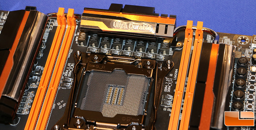
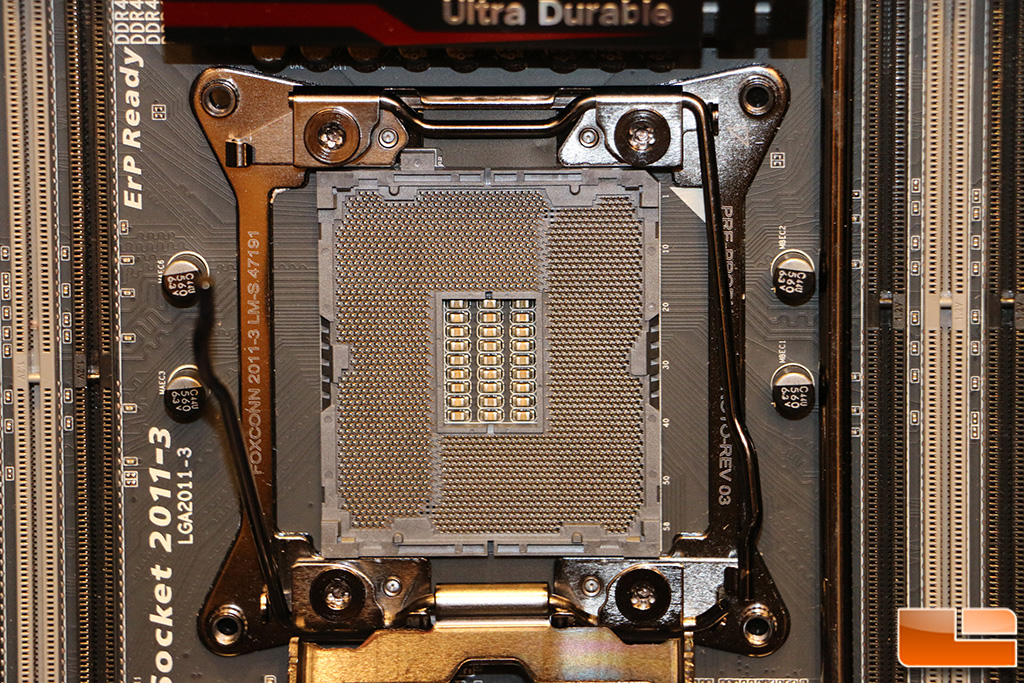
The most interesting thing about the Gigabyte GA-X99-SOC Force LN2 motherboard is the special LGA2011-v3 socket that is being used. Gigabyte went with a special CPU socket on this board that has more pins than a traditional socket. Gigabyte said that this has been shown to improve overclocking and they are trying it out on this board due to the fact that it is aimed at breaking overclocking records.
This socket looks very similar to the patent-pending ASUS OC Socket that ASUS is using on all of their X99 motherboards. From what we gather Intel had a number of pins on the Haswell-E processors for R&D testing purposes that weren’t needed for normal operation. Intel did not fuse off or internally disable the pads on the processor, so companies like ASUS and Gigabyte are now doing some reverse engineering and enabling their functionality. When ASUS first announced the OC socket there was some discussion if it would void Intel’s processor warranties, but it looks like it does not. We do know that Intel is actively looking into what the OC socket does as they didn’t plan on motherboard makers to come out with boards that have enabled more pins than planned. Intel could possibly make some changes down the road if needed. (Intel could easily fuse off and disable the pads at the package level on future processor production runs and just simply end these special socket boards if they wanted to do so).
Foxconn makes various Intel LGA2011-v3 sockets and there are different pin arrangements that can be ordered. It appears that companies like ASUS and Gigabyte are sourcing ‘special’ sockets from Foxconn and then enabling some of those extra pins on the board level. Supposedly having the extra pins allows for better uncore clock adjustments, which improve the CPU cache frequency. Intel is looking into what ASUS and Gigabyte are doing as they didn’t plan on motherboard makers to come out with boards that have enabled more pins than planned.
Will ASUS be able to get their patent approved? Will Gigabyte be getting sued by ASUS for using such a socket? Is the socket on the Gigabyte board even functional? We have no clue and thankfully aren’t lawyers! The ASUS fans are likely thinking that Gigabyte ripped off the ASUS design and that they cannot come up with anything on their own. Others will be thinking that Intel designed the processor and that Foxconn made the socket, so how can you patent something you didn’t make in the first place. If Gigabyte changed the pin-count by one would it be breaking the patent? We’ll let the the higher powers figure it out, but now both ASUS and Gigabyte are using LGA2011-v3 sockets with more pins that Intel planned for.
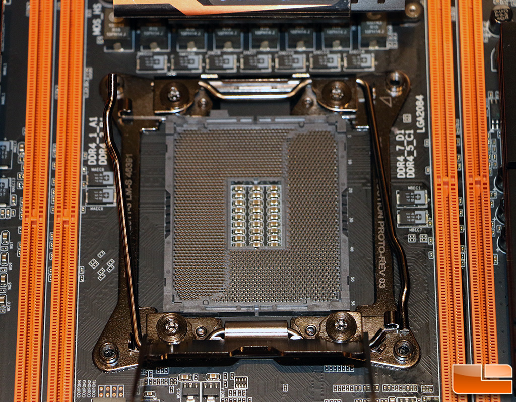
Here is a shot of the socket on the Gigabyte GA-X99-Gaming 5 motherboard that has fewer pins on it.