EVGA GeForce GTX 260 Core 216 Superclocked Video Card
NVIDIA Adds More Shaders to the GeForce GTX 260
A couple days ago the great and powerful forces over at NVIDIA launched a new graphics card called the GeForce GTX 260 Core 216. This new graphics card was launched to fill the gap between the GeForce GTX 260 and GeForce GTX 280. What gap might this be? It would be the gap where the ATI Radeon HD 4870 would be performing. By adding more shaders and increasing the MSRP by $50 the marketing team over at NVIDIA felt it made for a great new product and thus a card was born. This launch came to a shock as I didn’t know much about it till just a number of weeks before these cards launched and since we got our review sample the day the new GeForce GTX 260 Core 216 graphics cards launched it can be assumed that these were rushed to market very quickly. Another sign of this is that NVIDIA didn’t send out any reference cards and all the review samples were from add-in-board partners like the one we are looking at today from EVGA. You might be thinking how NVIDIA added more shaders to the GeForce GTX 260, so let’s answer that before moving on to the review.
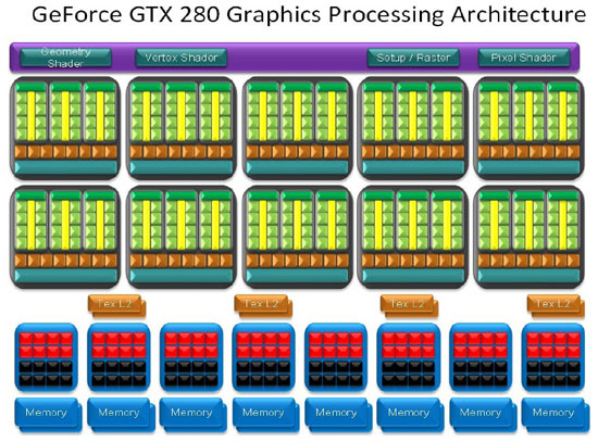
When the GeForce GTX 200 series originally launched I covered some of the basic processing architecture, so feel free to reference that article to get a feel for the GTX 200 series. The processing architecture of the GeForce GTX 280 video card has 240 shader processors that are arranged within 10 blocks of 24 as seen in the diagram above. Each of these blocks is called a TPC (Thread Processing Cluster) and is where the focus will be for this article. The GeForce GTX 280 offers a full 512-bit memory bus thanks to the eight 64-bit memory controllers that are also seen in the above image. In order to make a lower cost part that more people can afford, NVIDIA then made a part with less TPCs and memory controllers by disabling certain areas of the core. The result of ‘neutering’ the GTX 280 was the GTX 260 seen here.
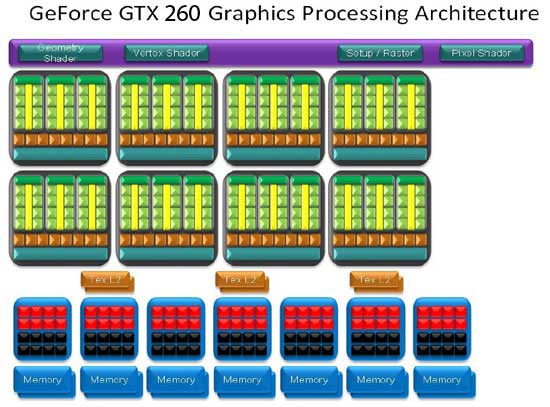
By removing a pair of the Thread Processing Clusters and one of the 64-bit memory controllers you end up with the GeForce GTX 260 that is on the market today. By removing/disabling these parts the GeForce GTX 260 has 192 shader processors and a 448-bit memory bus, which wasn’t enough to compete with the ATI Radeon HD 4870 graphics card that was right behind the GeForce GTX 280 in nearly all the benchmarks I tested it in.
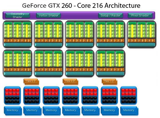
The quick and easy way to give the GeForce GTX 260 a performance boost was to enable/add one more Thread Processing Cluster, which contains 24 more shader processors. This gives the GeForce GTX 260 Core 216 a total of 216 shader processors and a new name. Since nothing was done with the memory controllers everything else on the card stays the same. What you end up with is card that offers a 448-bit memory bus and 896MB GDDR3 frame buffer just like the original GTX 260. The clock speeds also remain the same with the core clock at 576MHz, shaders at 1242MHz and the memory clock set to 999MHz. Pricing on a regular GeForce GTX 260 runs about $250 and one of these new Core 216 versions will set you back for about $300. Let’s take a look at the actual card that will be reviewed today.
Comments are closed.