DDR2 Memory: Enhanced Performance Profiles (EPP)
Slides 4 – 6
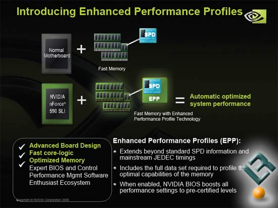
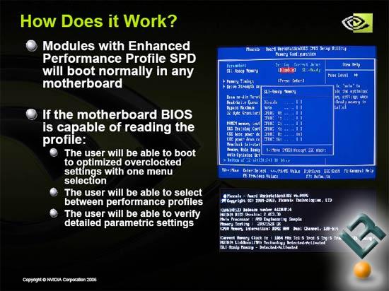
On slide number four we see that when memory modules have EPP programmed into the SPD that they will be automatically optimized for the highest level of memory performance if that option is set in the BIOS. The end user will be able to enable and disable the feature “SLI Memory” in the BIOS of many AMD AM2 boards that we have seen.
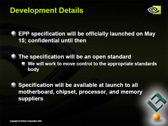
Slide five states that EPP will be launched on the 15th of May and will be an open standard for all to use. This means that ATI and VIA could use this technology on their future chipsets and any memory company can put EPP settings into their modules SPD at free will. Since AMD’s AM2 processors are not out yet any more information about motherboards and processors will have to wait.
For starters EPP is stored in the SPD between JEDEC Byte numbers 99 and 127, which is currently unused space on the majority of shipping memory modules. By placing information here in a consistent order (the EPP standard) and having a BIOS that knows to look at these Byte values for information you have EPP memory. This adds no new cost to the module as nothing on the PCB has been changed. EPP just takes advantage of dead space that you already paid for and inserts information to improve platform performance.
The EPP may contain up to two full performance profiles. The full profiles are very comprehensive, and are tailored towards modules where the highest degree of parametric specification is desired. The EPP may contain up to four abbreviated performance profiles. Some detailed parameters are not included in the abbreviated profiles; only the most commonly modified parameters are included. The abbreviated list of parameters allows four profiles to reside within the EPP, rather than just two.
Comments are closed.