An Overview of Intel’s Teraflops Research Chip
Intel Creates One CPU With 80-Cores at 4GHz Each

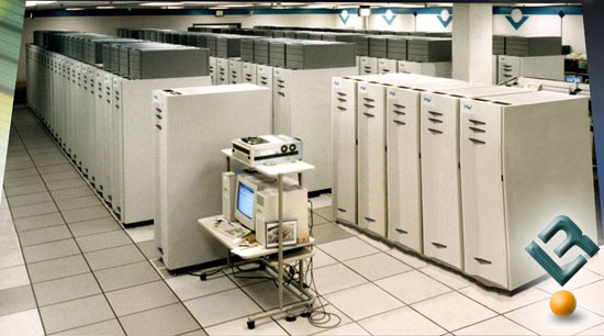
Over the weekend Intel announced that they were able to produce an 80-core processor that is able to do trillions of calculations per second. This would make it the World’s first programmable processor to deliver Teraflops performance! How does this new research chip change the future of processors? The first time Teraflops performance was achieved was in 1996, on the ASCI Red Supercomputer built by Intel for the Sandia National Laboratory. That computer took up more than 2,000 square feet, was powered by nearly 10,000 Pentium Pro processors, and consumed over 500 kilowatts of electricity.
That was then and this is now! Below is the first true image of the 80-core research chip that can do a Teraflop of performance while consuming only 62 watts – less than many single-core processors today.
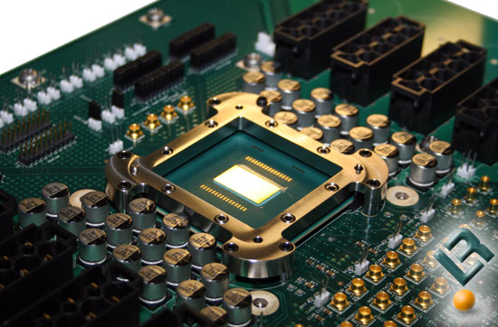
The board pictured above houses Intels 80-Core Teraflops Research Chip. Just ten years ago it took 10,000 Pentium Pro Processors to do the work that the 80-core processor above can do! What does the die of an 80-core processor look like?
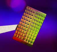
The above image is a close-up of an Intel Teraflops Research Chip wafer taken partway through the fabrication process to expose the cores. The ’tile-based’ design allows researchers to use smaller cores that can easily be repeated across the chip. A single-core chip of this size (100 million transistors) would take roughly twice as long and twice as many people to design. Each one of these cores contains two programmable floating point engines the most ever to be integrated on a single chip.
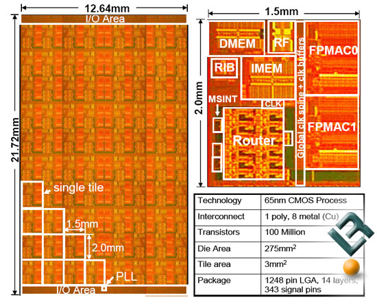
To better see the two floating point engines we can look at the full-chip and tile micrograph to see how each is designed. The entire 80-core processor was made on a 65nm CMOS process and has a die are of 275mm2. That means that each and every tile is just 3mm2! Don’t expect this prototype processor to fit in your current motherboard as it used a 1248-pin (LGA-1248) package design.
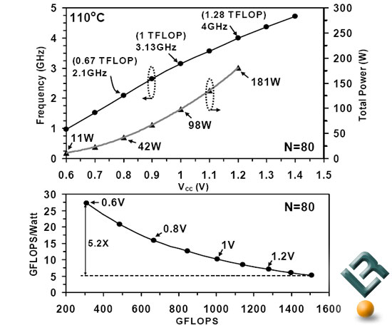
One of the most impressive areas on the 80-core processor is not the performance it has, but the low thermal package that it is reported to have. The above chart shows the estimated frequency and power versus Vcc, and power efficiency with all 80 tiles (N) active. Running on a 1.0v current at 110 degrees C the tile maximum frequency is 3.13 GHz while at 1.2v the tiles can run at 4.0 GHz. That brings the peak processing performance with all 80 tiles functioning on block matrix operations to 1.0TFLOPS at 1.0v and 1.28TFLOPS at 1.2v. Power consumption at these levels is estimated at 98W and 181W respectively.
While all this sounds great just remember that Intel has no plans to bring this processor to the market.
“Intel has no plans to bring this exact chip designed with floating point cores to market. However, the company’s Tera-scale research is instrumental in investigating new innovations in individual or specialized processor or core functions, the types of chip-to-chip and chip-to-computer interconnects required to best move data and most importantly, how software will need to be designed to best leverage multiple processor cores. This Teraflop research chip offered specific insights in new silicon design methodologies, high-bandwidth interconnects and energy management approaches.”
It seems that the ‘Era Of Tera’ is really on the way and hopefully sooner, rather than later, we will each have a Teraflop processor in our home computers!
Comments are closed.