AMD Phenom II X4 940 Processor Review
Same Architecture, New Process
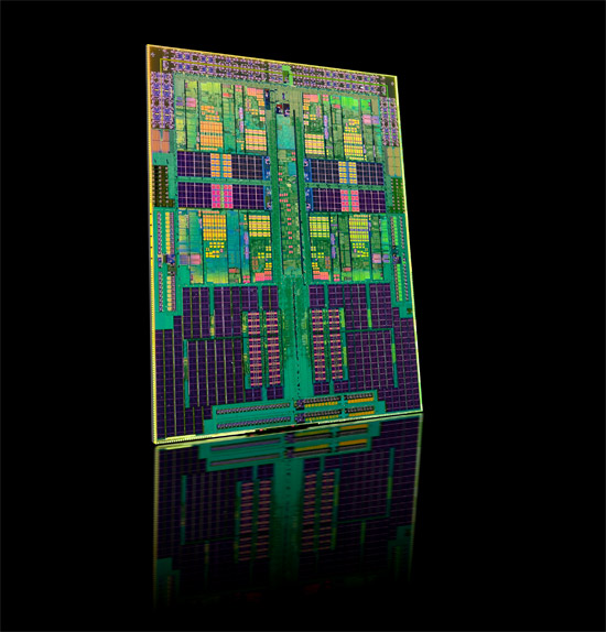
With everything looking so bright, the processor is rightly codenamed Deneb, which happens to be the 19th brightest star in the sky. Deneb looks to be a bright spot of light in a product lineup that has otherwise consisted of a lot of doom and gloom lately. Initial Deneb-based processors will launch on AMD’s AM2+ platform, feature DDR2 memory controllers, and a 125W TDP. Look out in the near future for the new AM3 platform with Deneb processors featuring hybrid DDR2/DDR3 memory controllers. AMD has been pushing the backwards compatibility of their entire lineup and while that hasn’t always been true, Deneb looks to at least hold some promise with AM3 chips working in AM2+ sockets and AM2+ chips being direct replacements for older Phenom and Athlon chips.

AMD has continued to develop their SOI (Silicon On Insulator) technology with their latest being a 45nm SOI manufacturing process. Judging from initial impressions, they have tweaked the process a bit so that it continues to scale with voltages unlike their 65nm process that often hit voltage scaling walls. Add to this the general improvements you get with a process shrink and Phenom II could potentially reverse the overclocking and power consumption stigma that Phenom had branded across AMD.
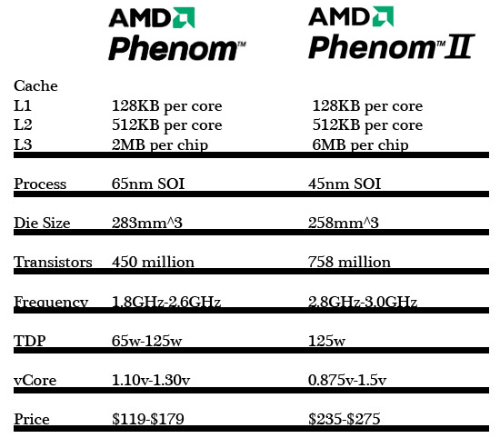
Below is a short list of differences between Phenom and Phenom II. Most notable are the launch frequencies, cache increases, and respective price jump. The Phenom II X4 940 I have here is a retail sample sent from AMD so it is retail quality silicon and should result in numbers that anyone can relate to. Unfortunately, I wasn’t given a retail heatsink but that doesn’t factor much into performance.


Comments are closed.