AMD High Bandwidth Memory Detailed With Joe Macri
AMD recently hosted a conference call on High Bandwidth Memory with Joe Macri that went gave more information about HBM and we wanted to share that information and the entire slide deck with our readers today. AMD believes that High Bandwidth Memory (HBM) interface is the right solution for their high-end Radeon R9 300 series video cards and will likely be rolling it out in the near future on APUs as well. This is new technology that you’ll want to know about and it won’t just be used by AMD. AMD and SKHynix worked together with a number of companies to help develop and set the HBM standard and HBM now has a JEDEC specification!
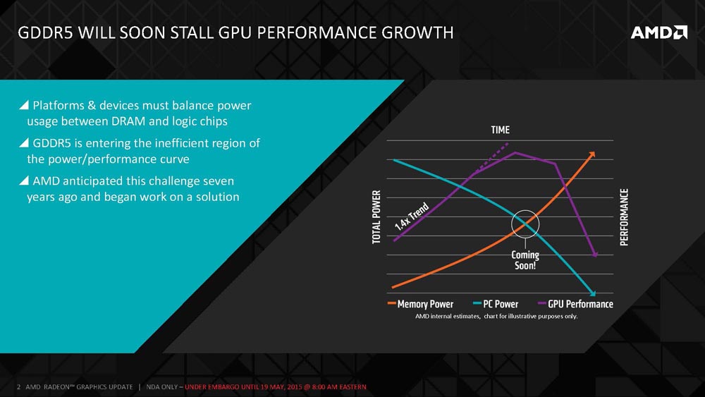
There were many challenges to bring HBM to market and the chart in the slide above was the image that AMD drew on the white board seven years ago to talk about what the next challenges were with regards to memory for GPUs. AMD saw that we are living in a power limited world and that as one sub system of the chip would go up in power that another would have to go down. The problem here is that the memory power for GDDR5 was ever increasing and there are only so many Watts that could be applied. AMD was able to look at memory bandwidth projections and see that down the road they wouldn’t be able to have the bandwidth needed if they kept headed down the GDDR5 path. AMD saw that bandwidth per watt was going to be a big challenge.
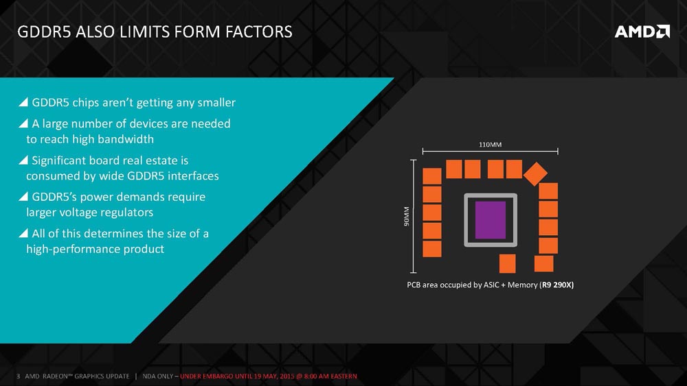
The other problem with GDDR5 memory is that form factors is another issue as devices are getting smaller, but the PCB area needed for the ASIC and memory for a graphics cards isn’t getting smaller. AMD saw this as an issue and started looking at the bandwidth per mm2 metric as they wanted to improve on this to help bring ‘incredible’ new video card form factors to market.
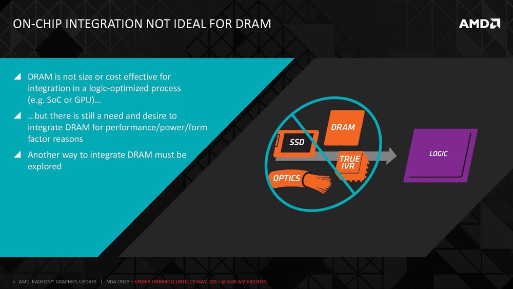
DRAM is note size or cost effective for integration in a SoC or GPU as they are optimized for the bit cells to hold a charge like a capacitor. You can implement logic, but the transistors act many generation older and merging the DRAM process with a logic process is tough to do and there are extra costs involved. AMD believes that this is the reason that embedded DRAM has never taken off and that keeping the DRAM seperate from your logic process is usually always the best choice.
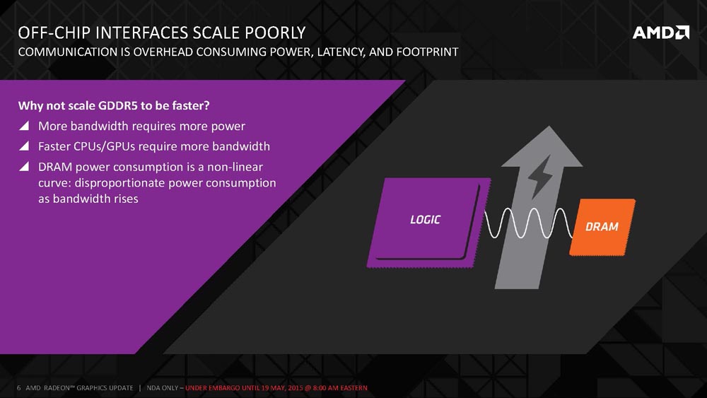
AMD looked at scaling GDDR5 faster, but while it might have worked for a period of time it still had big issues. They couldn’t reduce the footprint size, the asymmetrical memory interface design was causing increased latencies and it was using more and more power.
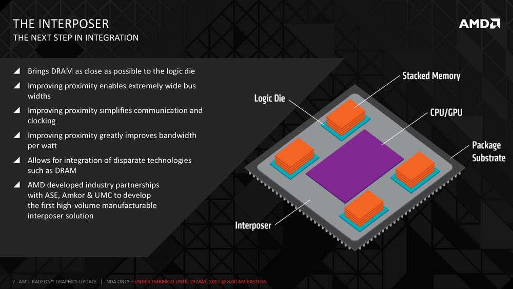
AMD decided to go another direction and looked at going wide and slow since they were just looking for bandwidth. In this particular case they also got improved latencies, which wasn’t their primary goal. AMD created a passive interposer that has no active transistors. This allows for incredible densities due to the closeness of everything. With this design AMD was able to go from 32-bit on GDDR5 memory to 1024-bit width bus on HBM. The interposer is built by UMC and uses an older technology as it doesn’t need to be made using the latest fab technology.
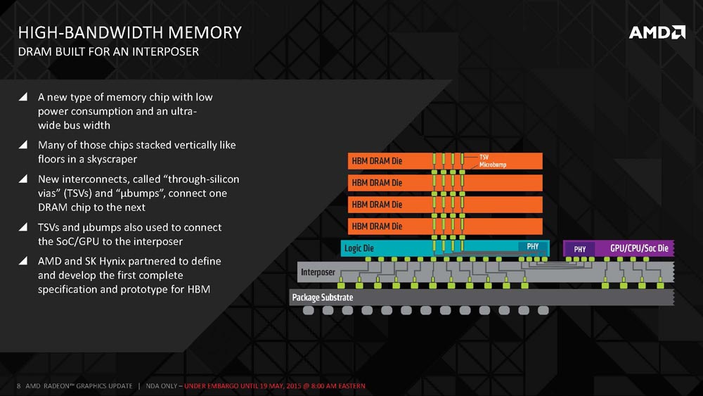
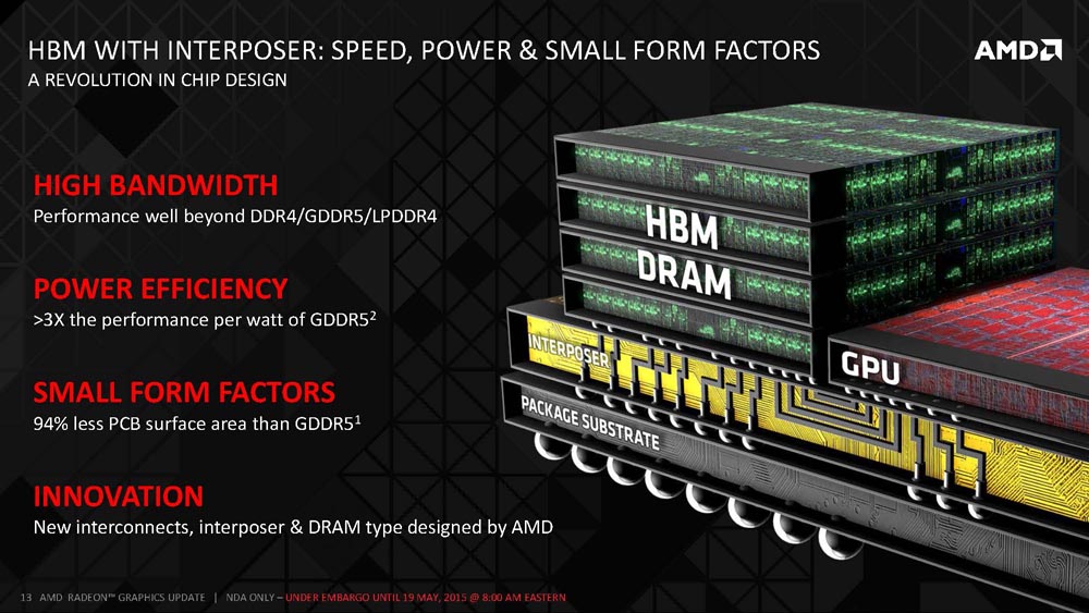
This slide hows the general HBM layout. On the bottom you have a standard organic package substrate that is now totally separated from the high-speed memory sub system. Above that you have the silicon interposer that obviously attaches to the to the package substrate on one side and then the HBM logic chip and GPU. HBM is designed as a true 3D design that is made up of four storage chips and one logic chip. The little green columns in the in the image above show Through Silicon via (TSV) interconnections. These are basically holes that are punched in the silicon of the HBM DRAM and Logic chips as well as the interposer. All five of these chips have TSV’s on them. When you are building one of these pieces of silicon they are just 100 microns thick! The interconnect between the DRAM stack and the discrete GPU is shown on the PHY blocks on the edges of the chips.
The PHY’s are laid out on the edges of the chips to keep the latency to a minimum. HBM does decrease the latency as data is for the most part no longer being moved horizontally to a central part of the die like it was with GDDR5. With HBM it is pushed down vertically and that really helps reduce the latency. HBM has more channels and banks and that helps improve pseudo random access, which is critical to reducing latency for the HPC market.
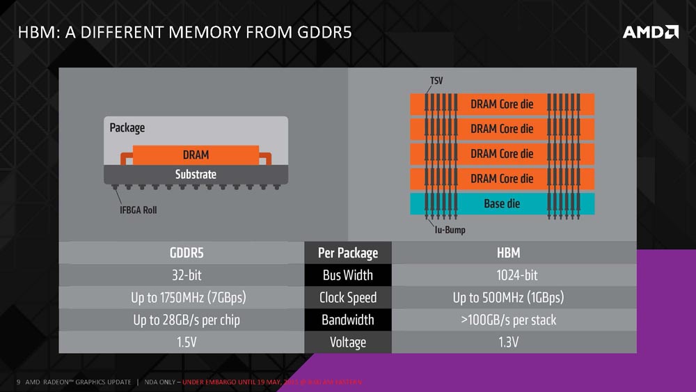
This slide compares GDDR5 to HBM as you need to compare things differently since we have gone to the 3D space and are no longer 2D planer. As mentioned a few slides ago the bus width has gone from 32-bit to 1024-bit and the clock speed has gone from 1750MHz (7GBps) to 500MHz (1GBps). This is much slower, but they can get away with with it by having such a wide bus. By only running at 500MHz it means that AMD can also utilize much simpler clocking methods with no terminators needed for this interface. Simple clocking also means that this is a low power solution as it needs just 1.3V versus 1.5V. Bandwidth has gone from 28GB/s to 128GBs/s, so there is a massive bandwidth improvement that will be had by going from GDDR5 to HBM. Each Gen 1 HBM is capable of 128 GB/s per stack and there are four devices in each package. Each stack offers 1GB of storage space, so that means they first video cards using this technology will have 4GB of HBM memory. Moving to Gen 2 HBM will basically double performance, so things will only be getting better. AMD isn’t discussing how much the latency was reduced as they want to keep the memory subsystem under wraps so competitors have to figure it out themselves.
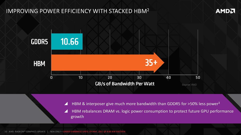
So when it comes to GB/s of bandwidth per watt has gone from 10.66GB/s to over 35GB/s and this is with HBM1, not the newer HBM2 technology.
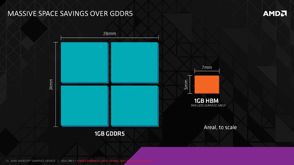
AMD has a massive area reduction with HBM as they went from 672mm2 with a 1GB GDDR5 solution to just 35mm squared for a 1GB HBM Stack. This is a 19x reduction in the surface area for the same amount of DRAM.
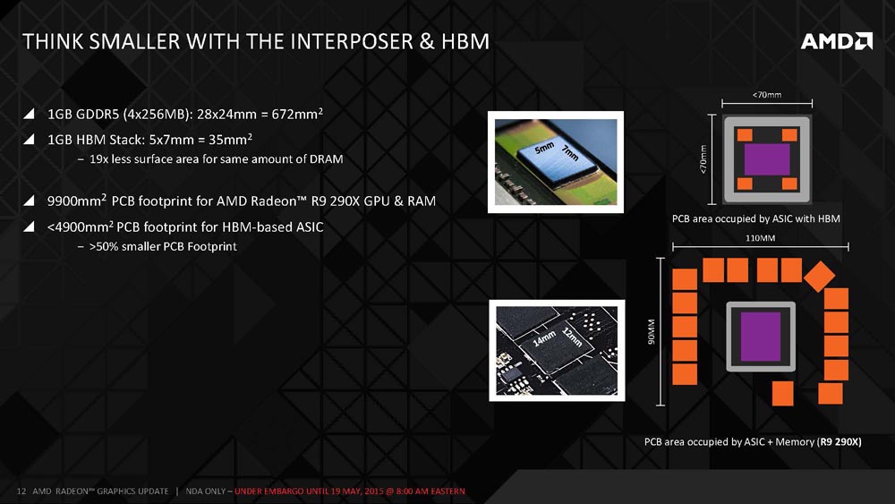
The overall PCB footprint for the AMD Radeon R9 290X video card is 9,900mm2 when you measure the area occupied by both the ASIC and memory. AMD says that footprint can be reduced to less than 4900mm2 with an HBM-based ASIC. This is greater than a 50% reduction in the overall PCB footprint and opens up a ton of board real-estate. This means that smaller form factors will be possible. AMD told Legit Reviews that the savings are actually greater than shown in this illustration as there is space savings to be had in the power subsystem since lower power subsystems require less space as well.
AMD believes that HBM will allow them to bring performance to places that they have never done before. AMD was able to pull this off with a large ecosystem and it took a large number of test chips to pull this off over the past seven years. SKHynix was the major contributor on the DRAM side.
HBM isn’t just for graphics cards though as AMD sees benefits will be had by HBM in the HPC, APUs, switches, printers, high-speed professional cameras and so on. From what we gather AMD will introducing HBM memory on couple a high-end desktop graphics card like the AMD Radeon R9 390X and R9 390. This won’t be used on a top to bottom product offering, which might cause some to wonder how cost effective this will be to do since it obviously won’t be a super high volume card. AMD said that is nothing to be concerned with as when GDDR5 was first introduced things were done very similarly and everything turned out okay. AMD’s RV770 GPU (Radeon HD4850 and Radeon HD 4870) was the first in the world to feature a 256-bit memory controller and is the Radeon H 4870 was unique in the sense that was the first GPU to support GDDR5 memory. The memory on the Radeon HD 4870 back in June 2008 was running at 900 MHz giving an effective transfer rate of 3.6 GHz and a memory bandwidth of up to 115.2 GB/s. AMD sees HBM moving into the discrete graphics card line and well beyond just GPUs if you look far enough out. AMD will use HBM where it makes sense and they feel that they will be the most aggressive with this technology and feels that they are a year ahead of their competition (NVIDIA) right now.
One of the final comments made by Joe Macri was that the end user places value on performance, form factor and power. Those are areas that AMD is arguably loosing to NVIDIA right no on the high-end, so we can’t wait to see how the new cards perform and to see if AMD can take the lead in new areas.