NVIDIA Announces CUDA GPU Architecture – Fermi
Finally an Update on GT300 – Fermi
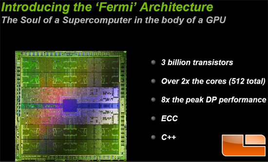
NVIDIA today introduced its next generation CUDA GPU architecture, codenamed Fermi at the GPU Technology Conference in San Jose, California. Fermi is entirely new from the ground-up design architecture and is said to be the foundation for the worlds first computational graphics processing units (GPUs), delivering breakthroughs in both graphics and GPU computing.

It is completely clear that GPUs are now general purpose parallel computing processors with amazing graphics, and not just graphics chips anymore, said Jen-Hsun Huang, co-founder and CEO of NVIDIA.

With that Jen-Hsun Huang laid out what he considers the soul of the Supercomputer in the body of the GPU. With ~3 billion transistors he really isn’t kidding as this is one large GPU that should have a ton of processing power.

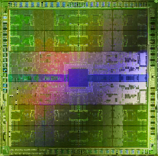
Here is a better shot of the new Fermi die. The massive die that is made by TSMC has been made up of 3.0 billion transistors and features 512 CUDA processing cores that are organized into 16 streaming multiprocessors of 32 cores each. The memory architecture is built around a new GDDR5 implementation and has six channels of 64-bits for a total memory bus of 384-bits. The memory system can support up to 6GB of memory and rumor has it, one card will actually feature 6GB of memory! With Fermi, NVIDIA has focused a ton of time and effort on things like double precision floating point, ECC support of the memory caches and context switching between GPU applications, which are all important in parallel computing.

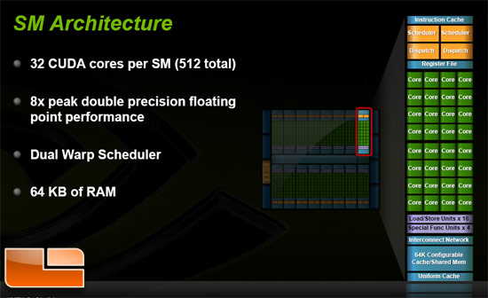
Each SM includes 32 CUDA processing cores (4x the previous GT200 design) as you can see above. This means that the peak double precision floating point performance has more than eight fold increased this time around. The GPU also supports the IEEE 754-2008 standard, which is said to be important for GPU computing.

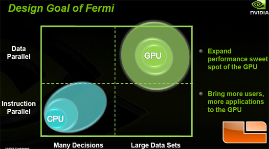
This slide shows that the design goal of Fermi was to basically expand the performance sweet spot of the GPU in order to increase the number of users and applications of the GPU. Fermi isn’t all about gaming performance and is clearly more aimed at a better computing experience, rather than just a better gaming experience. That being said NVIDIA also stated that it would be faster than what ATI launched last week. They would be referring to the ATI Radeon HD 5870 graphics card for those that haven’t been keeping up on their news. NVIDIA didn’t give a launch date other than saying it would be released on an upcoming Tuesday. They also wouldn’t talk about performance with the exception of saying that it was faster than the Radeon HD 5800 series when it comes to gaming.
Let’s take a look at a graphics card that is running a Fermi GPU!

Comments are closed.