Toshiba Highlights Industry Firsts at Flash Media Summit
Toshiba Highlights Industry Firsts at Flash Media Summit
This week at the 10th Anniversary Flash Memory Summit in Santa Clara, California, Toshiba will be showcasing its latest memory and storage solutions including two world firsts: a 16-die stacked NAND flash memory utilizing TSV (Through Silicon Via) technology; and its 256Gb, 48-layer BiCS FLASH.
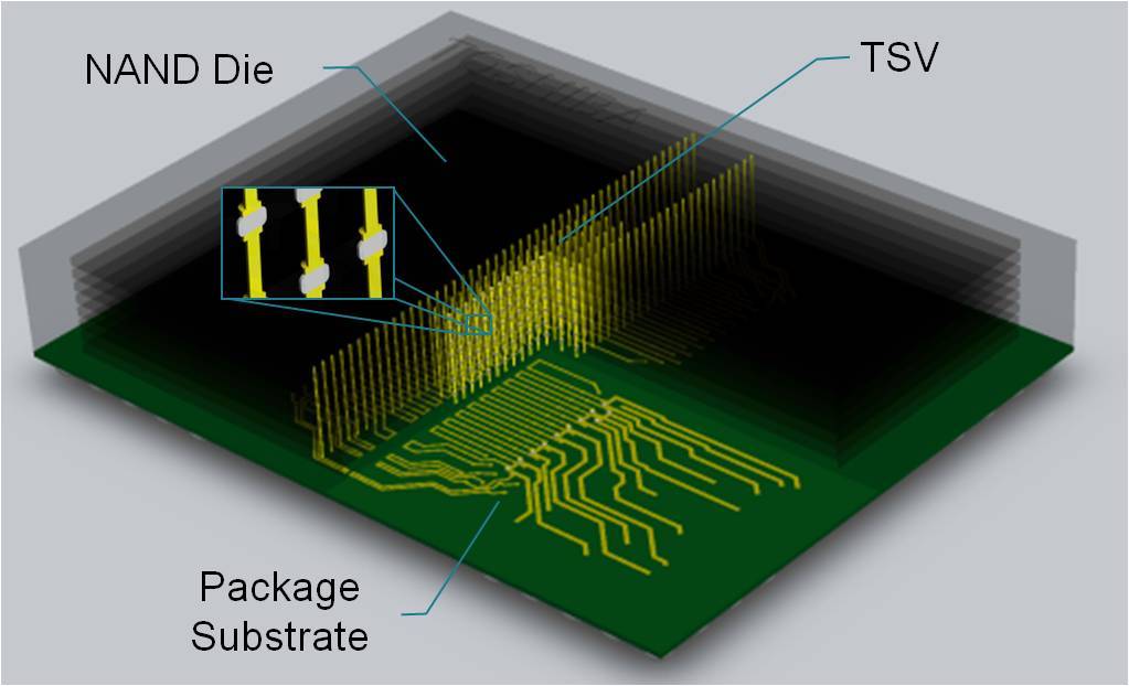
Toshibas new NAND flash memory with TSV provides an ideal solution for low latency, high bandwidth and high IOPS/Watt in flash storage applications, including high-end enterprise SSDs. Through Silicon Via, or TSV, is a vertical electrical connection (via) passing completely through a silicon wafer or die.
A 3D stacked cell structure flash memory, Toshibas BiCS FLASH is based on a leading-edge 48-layer stacking process that surpasses the capacity of mainstream two dimensional NAND flash memory, while enhancing write/erase reliability endurance and boosting write speeds.
Posted below is the official press release from Toshiba’s website:
Toshiba Develops World’s First 16-die Stacked NAND Flash Memory with TSV Technology
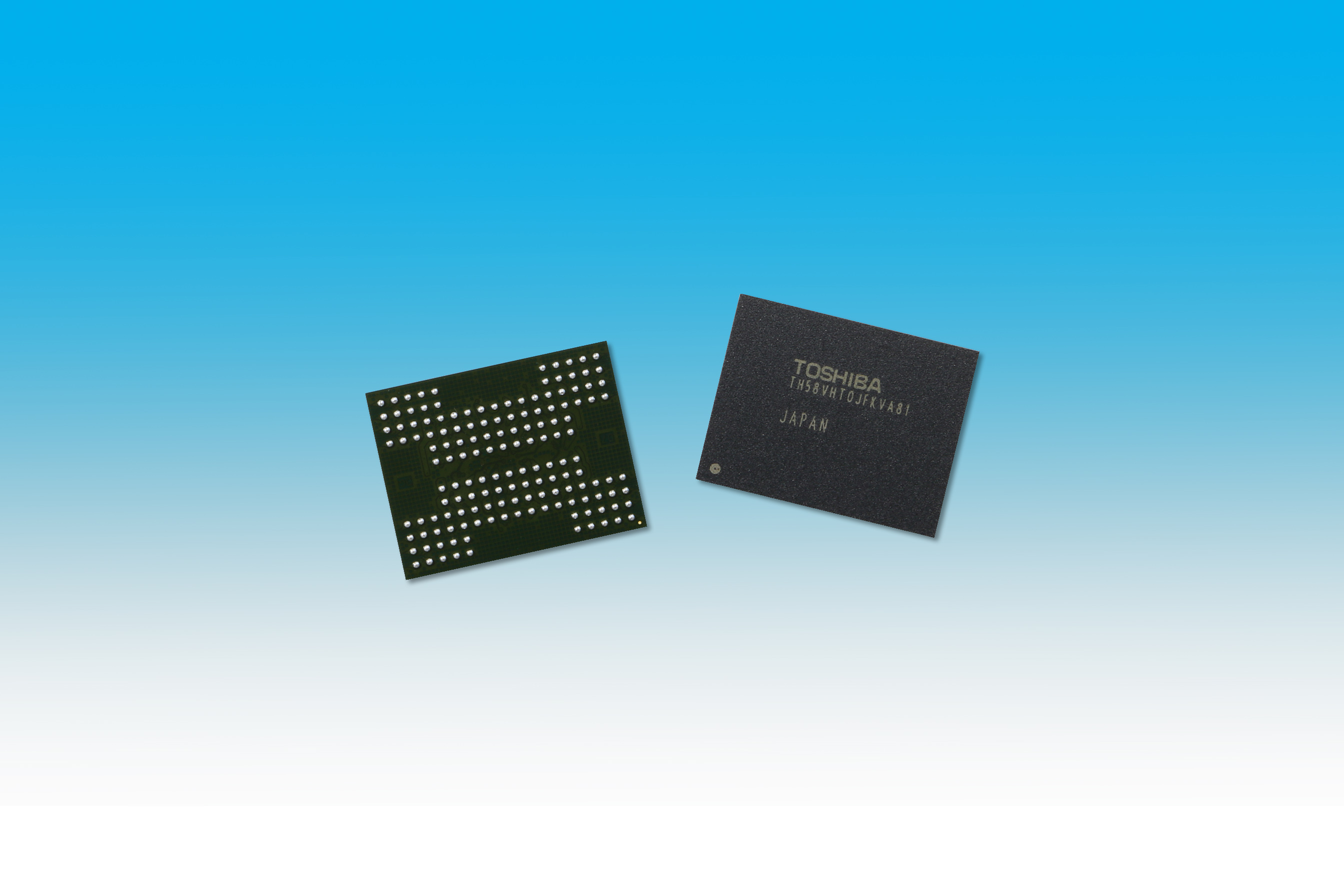
TOKYO–Toshiba Corporation (TOKYO:6502) today announced the development of the worlds first*1 16-die (max.) stacked NAND flash memory utilizing Through Silicon Via (TSV) technology. The prototype will be shown at Flash Memory Summit 2015, to be held from August 11 to 13 in Santa Clara, USA.
Committed to People, Committed to the Future
The prior art of stacked NAND flash memories are connected together with wire bonding in a package. TSV technology instead utilizes the vertical electrodes and vias to pass through the silicon dies for the connection. This enables high speed data input and output, and reduces power consumption.
Toshibas TSV technology achieves an I/O data rate of over 1Gbps which is higher than any other NAND flash memories with a low voltage supply: 1.8V to the core circuits and 1.2V to the I/O circuits and approximately 50%*2 power reduction of write operations, read operations, and I/O data transfers.
This new NAND flash memory provides the ideal solution for low latency, high bandwidth and high IOPS/Watt in flash storage applications, including high-end enterprise SSD.
A part of this applied technology was developed by the New Energy and Industrial Technology Development Organization (NEDO).
The General Specification of Prototype
Package Type NAND Dual x8 BGA-152 Storage Capacity (GB) 128 256 Number of Stacks 8 16 External Dimension (mm)
W 14 14 D 18 18 H 1.35 1.90 Interface Toggle DDR Note:
*1: As of August 6, 2015. Toshiba survey.
*2: Compared with Toshibas current products.