SanDisk Ultra II 240GB SSD Review – SanDisk’s First TLC NAND SSD
A Closer Look at the SanDisk Ultra II:
Opening the drive consisted of the removal of four screws, each of which were located under the sticker on the back of the drive making removal without detection near impossible. A thermal pad resides on the back plate which covers all of the components on the controller side of the PCB.
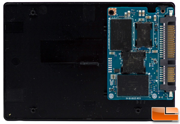
The PCB is tiny in comparison to the overall drive size. It’s like buying a bag of potato chips (or crisps for you folks across the pond).
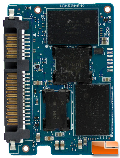
One one side of the PCB we find just two NAND modules.
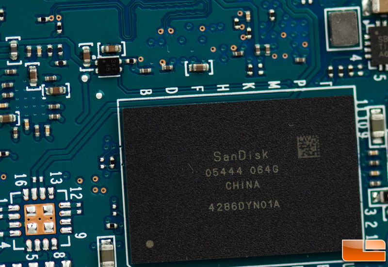
A closer look at the NAND reveals SanDisk branding and part number 4286DYN01A. This is TLC 19nm toggle NAND which we spoke about in more detail on the opening page. There are only four total packages on the board, each with a density of 64GB.
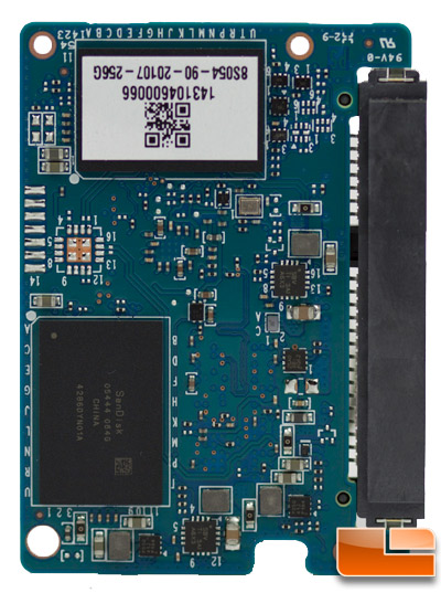
Flipping the board over we see more of the NAND, the cache and the controller. Apologies for the lint on the chips, it was left there in the attempt to wipe off the residue left behind by the thermal pad.
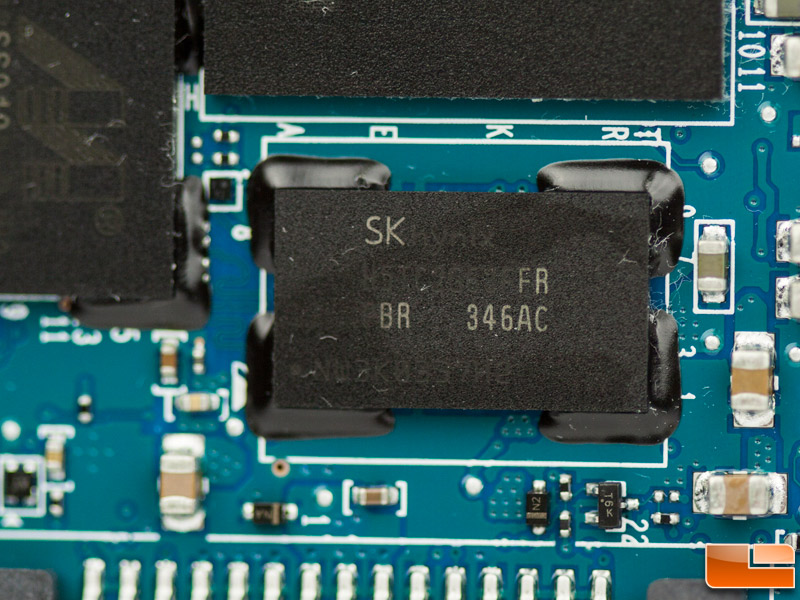
The SK Hynix DDR3 SDRAM cache is labeled as H5TC2G63FFR and is 256MB in capacity.
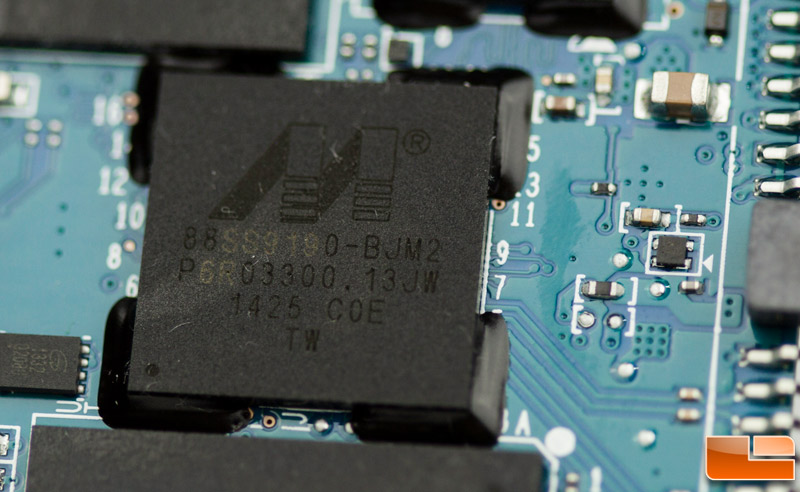
The Marvell 88SS9190 controller is new and the info we have on it is not very robust. From what we’ve been able to discern, it’s roughly the same as the Marvell 88SS9189 controller except is has four channels, not eight. This makes sense since there are only four NAND packages on board and we are told the higher capacity drives use the Marvell 88SS9189 controller as they can leverage more of the channels. The controller handles all the usual duties and runs a SanDisk custom firmware that does not support encryption or the newer DevSleep function although neither will probably be missed – especially in a budget friendly drive.