NVIDIA GP100 Pascal GPU Announced – 15 Billion Transistors, 21 FP16 TFLOPS, HBM2, 16nm FinFET
NVIDIA has unveiled the Tesla P100 datacenter GPU that utilized the companies new flagship GP100 Pascal GPU. NVIDIA said that the GP100 GPU measures in at 610mm2 and features 15.3 billion transistors. This makes it the largest GPU that NVIDIA has ever made despite the fact that it is built using the 16nm FinFET manufacturing process. It features 56 SMs and 3,584 CUDA cores that have a base clock of 1328MHz and a boost clock of 1480MHz. When it comes to compute performance NVIDIA said that it features 5.3 TFLOPS double precision FP64, 10.6 TFLOPS single precision FP32 and 21.2 TFLOPS of half precision FP16 compute.
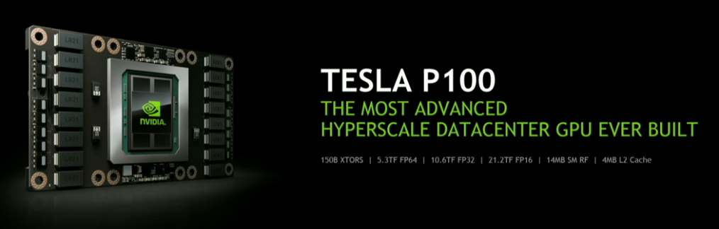
The GP100 GPU has has 4MB of L2 cache and 14MB of shared memory for just the register file due to how fast it’s able to crunch data. This GPU is targeted at hyperscale data center workloads. NVIDIA said that the Tesla P100 features 16GB of HMB2 memory! The 16GB of HBM2 memory runs on a 4096-bit bus and has 720 GB/s peak bandwidth.
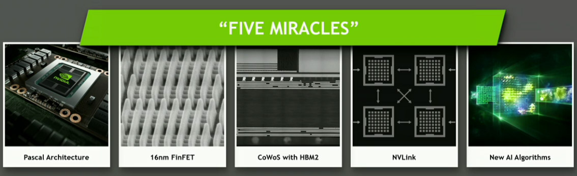
The GP100 GPU used in Tesla P100 incorporates multiple revolutionary new features and unprecedented performance. Key features of Tesla P100 include:
- Extreme performancepowering HPC, deep learning, and many more GPU Computing areas;
- NVLink NVIDIAs new high speed, high bandwidth interconnect for maximum application scalability;
- HBM2Fastest, high capacity, extremely efficient stacked GPU memory architecture;
- Unified Memory and Compute Preemptionsignificantly improved programming model;
- 16nm FinFETenables more features, higher performance, and improved power efficiency.
NVIDIA has a developer blog up about the GP100 that is worth a look. Here is a small section:
The Pascal GP100 Architecture: Faster in Every Way
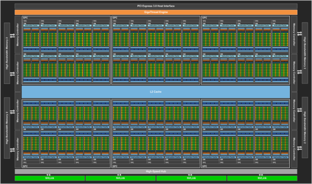
With every new GPU architecture, NVIDIA introduces major improvements to performance and power efficiency. The heart of the computation in Tesla GPUs is the SM, or streaming multiprocessor. The streaming multiprocessor creates, manages, schedules and executes instructions from many threads in parallel.
Like previous Tesla GPUs, GP100 is composed of an array of Graphics Processing Clusters (GPCs), Streaming Multiprocessors (SMs), and memory controllers. GP100 achieves its colossal throughput by providing six GPCs, up to 60 SMs, and eight 512-bit memory controllers (4096 bits total). The Pascal architectures computational prowess is more than just brute force: it increases performance not only by adding more SMs than previous GPUs, but by making each SM more efficient. Each SM has 64 CUDA cores and four texture units, for a total of 3840 CUDA cores and 240 texture units.
Delivering higher performance and improving energy efficiency are two key goals for new GPU architectures. A number of changes to the SM in the Maxwell architecture improved its efficiency compared to Kepler. Pascal builds on this and incorporates additional improvements that increase performance per watt even further over Maxwell. While TSMCs 16nm Fin-FET manufacturing process plays an important role, many GPU architectural modifications were also implemented to further reduce power consumption while maintaining high performance.
The following table provides a high-level comparison of Tesla P100 specifications compared to previous-generation Tesla GPU accelerators.
Tesla Products Tesla K40 Tesla M40 Tesla P100 GPU GK110 (Kepler) GM200 (Maxwell) GP100 (Pascal) SMs 15 24 56 TPCs 15 24 28 FP32 CUDA Cores / SM 192 128 64 FP32 CUDA Cores / GPU 2880 3072 3584 FP64 CUDA Cores / SM 64 4 32 FP64 CUDA Cores / GPU 960 96 1792 Base Clock 745 MHz 948 MHz 1328 MHz GPU Boost Clock 810/875 MHz 1114 MHz 1480 MHz FP64 GFLOPs 1680 213 5304[1] Texture Units 240 192 224 Memory Interface 384-bit GDDR5 384-bit GDDR5 4096-bit HBM2 Memory Size Up to 12 GB Up to 24 GB 16 GB L2 Cache Size 1536 KB 3072 KB 4096 KB Register File Size / SM 256 KB 256 KB 256 KB Register File Size / GPU 3840 KB 6144 KB 14336 KB TDP 235 Watts 250 Watts 300 Watts Transistors 7.1 billion 8 billion 15.3 billion GPU Die Size 551 mm 601 mm 610 mm Manufacturing Process 28-nm 28-nm 16-nm [1] The GFLOPS in this chart are based on GPU Boost Clocks.