NVIDIA GF100 Fermi Architecture and Performance Preview
GF100 Fermi Details Emerge
Without a doubt one of the most highly anticipated releases for 2010 will be the NVIDIA GF100 Fermi graphics card. This DirectX 11 video card is coming to market late and has given AMD a pretty significant head start as the company recently announced that they have sold over two million DirectX 11 graphics cards. For nearly a year NVIDIA has told the media and their fans that GF100 is coming and that it will be the best performing graphics card that the world has ever seen. We last heard some details on the architecture on the graphics card back in September 2009 during the NVIDIA GPU Technology Conference. It was during this time that we learned it was called ‘Fermi’ and would contain an amazing 3 billion transistors. That is significantly more than its direct competition, the ATI Radeon HD 5870, as it has just 2.15 billion transistors. The thought of a graphics card that can destroy the Radeon HD 5870 graphics card has really built up the anticipation for GF100 to come to market. NVIDIA also helped build the hype by releasing little pieces of information about GF100 on social networking sites the past few months.
- GF100 is the codename for the first GeForce GPU based on the Fermi architecture!
- GF in GF100 stands for Graphics Fermi not GeForce!
- The GF100 board is 10.5-inches long — the same length as GeForce GTX 200 Series graphics cards!
- GF100 packs in over 3B (billion!) transistors!
- The GF100 supports full hardware decode on the GPU for 3D Blu-Ray!
- GF100 graphics cards will provide hardware support for GPU overvoltaging for extreme overclocking!
- GF100 supports a brand new 32x anti-aliasing mode for ultra high-quality gaming!
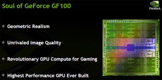
Legit Reviews was recently invited to take part in a media event that would allow a closer look at GF100 and we jumped at the chance to take a closer look at this 3 billion transistor beast. What we got was nearly an 8-hour long ‘deep dive’ into the architecture of the GF100 and other areas of interest such as game development, image quality, tessellation and a look at some demos that will be included in future power packs. We weren’t given any information as to when the GF100 graphics cards would be launched, what the clock frequencies will be, how much power they consume, what the real name will be or what the card will cost. So, what did we get? Let’s read on to find out.
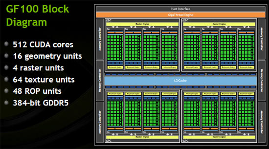
NVIDIA has gotten nailed by the media and consumers as ‘re-launching’ the same core with different clock frequencies and names for quite some time now. With the new core they have designed for GF100, NVIDIA went back to the drawing board and came up with a totally new design. The new die is being made by TSMC on what we believe is the 40nm manufacturing process. As previously noted it will have ~3.0 billion transistors and a total of 512 CUDA processing cores that are organized into 16 streaming multiprocessors of 32 cores each. The memory architecture is built around a new GDDR5 implementation and has six channels of 64-bits for a total memory bus of 384-bits. The memory system can support up to 6GB of memory and rumor has it one card will actually feature 6GB of memory!
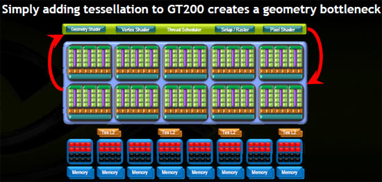
The new core design was developed with the future in mind as the current GT200 design doesn’t do too well with tessellation as it develops a geometry bottleneck.
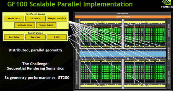
NVIDIA has spent a ton of time and developed a new scalable parallel implementation that greatly improves geometry performance thanks to the key placement of PolyMorph and Raster engines.
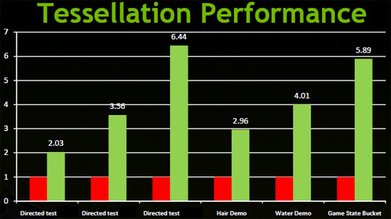
NVIDIA claims that the end result is that their GF100 has much better tessellation performance than ATI’s Radeon HD 5870 graphics card. How could this be? Let’s take a closer look at the architecture and find out.

Comments are closed.