Intel Broadwell Architecture Preview – Intel Core M and Broadwell-Y
Broadwell Architecture – 2nd Gen FIVR, 3DL, PCH
We were able to chat with Stephan Jourdan, Intel Fellow and Director of SoC Architecture at Intel about the microarchitecture changes that were done to Broadwell-Y.
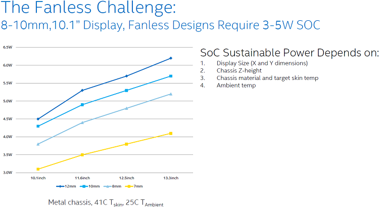
The goal with Broadwell-Y was to make a 8-10mm thick device with a 10.1″ display that was fanless with a 3-5 Watt SoC. Intel needed to optimize the CPU, GPU, PCH and move on to the 14nm process to create a sub-5 Watt SOC that could fulfill such a role.
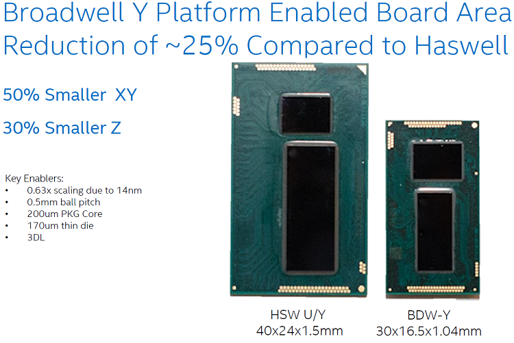
One of the key features of Broadwell Y is that the SoC is significantly smaller than Haswell U/Y. The Broadwell dies size is about 0.63x smaller than Haswell, so the die size is going from 130 mm^2 to 82mm^2. The overall package size for Haswell U/Y is 40x24x1.5mm and Broadwell will be 30x16x1.04mm. Broadwell-Y was originally designed to be 1.1mm in thickness, but Intel was able to exceed that goal and get it down to 1.04mm. On Haswell the packaged core was 400um in thickness, but on Broadwell it is just 200um.
The PCH is still made on the 32nm process, which is why the PCB size hasn’t changed much between Haswell and Broadwell. Intel has made changes to the PCH and it is a new design though, so consider it new as well.
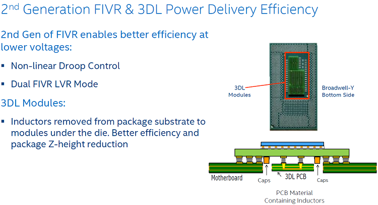
Intel is introducing 2nd Generation Fully-Integrated Voltage Regulator (FIVR) & 3DL for increased power delivery efficiency and performance with Broadwell-Y. The FIVR design requires external inductors to be placed on the bottom of the package and the height of the inductors was keeping Intel from going as thin as they wanted. Intel engineers and architects came up with something called the 3DL PCB. It is basically an external PCB for the inductors that mounts below the SoC and in a cutout in the board that the SoC is being attached to. This cuts the z-height of the Broadwell-Y SoC by almost half of what it was on Haswell-Y. This design was a major breakthrough when it came to thickness. Intel also improved the low voltage performance of FIVR by adding something called Dual FIVR LVR Mode, which from what we have been told, allows for the bypass of FIVR if needed.

Fueled by the desire to go fanless, the team at Intel also needed to play around with the way Turbo Boost is handled. Intel now has three power limit settings that allow for safe Turbo Boost operations. Haswell had just two power states. The new PL3 state allows for greater turbo boosting than ever before, but only for a very limited period of time. Intel said that the PL3 mode will last just milliseconds and is mainly there for battery protection as you wouldn’t want a SoC to try and pull more power than any given battery can safely deliver.
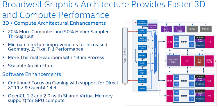
Intel also improved both Intel HD Graphics performance and efficiency. Broadwell-Y uses 24 Execution Units (EUs) which is 20 percent higher than the 20 EUs found in Haswell SoCs. Intel is still happy with this scalable architecture and is continuing to support gamers with quarterly driver releases and support for DirectX 11.2 and OpenGL 4.3. On the GPU Compute side you’ll have Open CL 1.2 and 2.0 with shared virtual memory support. Intel has also doubled the video quality engine throughput and improved the quality and performance for Intel Quick Sync Video Technology. The Intel HD Graphics in Broadwell will support 4K and Ultra HD displays on one monitor, but we aren’t sure about support for multiple 4K displays at this time. Native support for 4K wasn’t supported on the last generation Haswell Y or U processors as they supported displays up to 2560×1600. Intel said that they are able to support just 30 Hz refresh rates at 4K, so this is a baby step in the right direction. We were also told that H.265 video is supported and that 4k 30FPS encoding isn’t a problem.
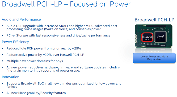
Intel made significant changes to the PCH with regards to power consumption when Haswell was released and everyone was impressed that the were able to accomplish. Many weren’t sure how many optimizations could be down to reduce power consumption on the PCH for Broadwall-Y, but it appears there were still more than could be done. Intel was able to add more power gating and was able to further reduce idle PCH power consumption by roughly 25 percent from the prior year. Intel was also able to reduce the active power use down by about 20 percent than the Haswell PCH-LP. Intel has also included hardware, firmware and software updates to introduce or improve the monitoring and reporting of power usage in the PCH. Intel hasn’t revealed specifics on all the Broadwell PCH-LP features just yet, but did note that the Audio DSP is being upgraded with increased SRAM and higher MIPS. This was done to improve power, but also helps with post processing and voice commands that can wake up a device with a keyword or phrase.
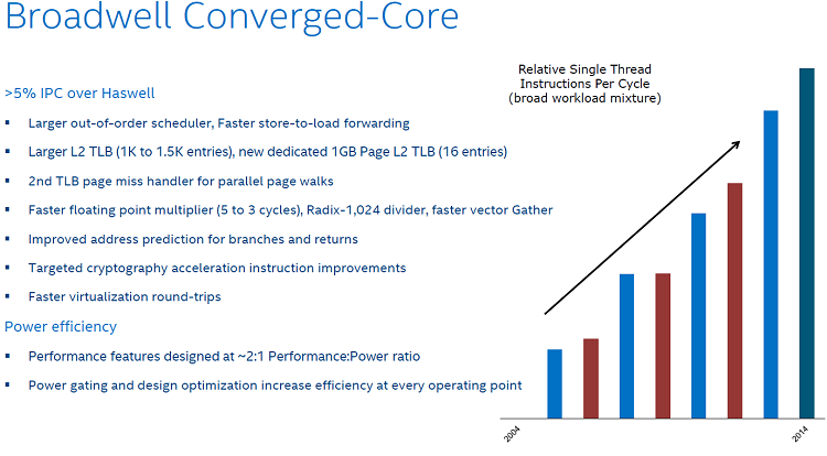
The slide above shows the only look at Broadwell performance, so be sure to take a closer look at it. Intel claims that the new ‘converged-core’ design in Broadwell will offer greater than five percent higher Instructions Per Cycle (IPC) when compared to Haswell. It doesn’t appear that there are any major instruction set changes for Haswell, but there were obviously a number of performance optimizations to get the mentioned gain. Some of changes include a Larger Out-of-Order scheduler for faster Store-to-Load forwarding, a Larger L2 TLB (1k to 1.5k entries) that has dedicated 1GB Page L2 TLB (16 entries) and more. Intel noted that the performance features were designed at ~2:1 Performance:Power ratio, which is the more aggressive than the 1:1 ratio that was targeted in previous processors.
Quick Summary:
It looks like Intel has been busy innovating on all fronts and the move to 14nm along with the introduction of Broadwell SOCs should be an exciting time for everyone. We can’t wait to see products powered by Broadwell-Y before the holiday!