HIS Radeon HD 4870 CrossFire Video Card Review – GDDR5 Arrives
Under The Heat Spreader
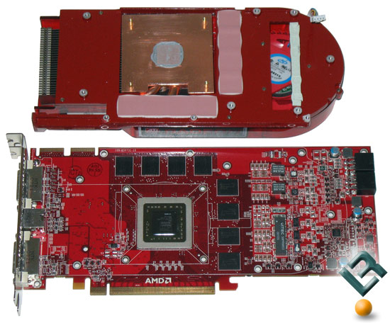
With the cooler and heat sink removed we can see the layout of the Radeon HD 4870. The heat sink is Copper and features two heat pipes that are used to transfer heat quickly to the aluminum fins. Notice the PCB says AMD on it this time around.
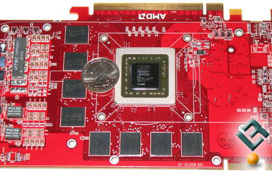
Here is a shot of the die and memory chips with a U.S. quarter (25 cent piece) to give you an idea of just how big the memory ICs are and the die.
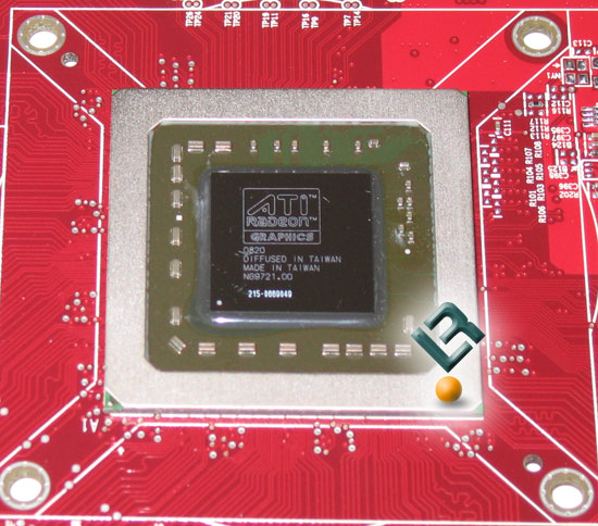
Here is a closer look at the die for those that want to look at what numbers are on our review sample. This particular core was made the 20th week of 2008 and was diffused and made in Taiwan.
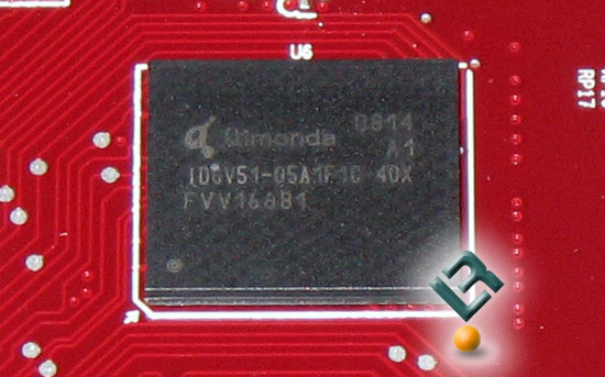
The Radeon HD 4870 is the first retail graphics card to use GDDR5 memory and the 512MB of memory uses Qimonda branded ICs. GDDR5 introduces features and functions that go beyond previous GDDR standards and enables GDDR5 to operate at data rates up to 6 Gbps, three times the performance of todays high speed GDDR3. The memory ICs feature adaptive power management, error compensation, adaptive interface timings and date eye optimization. The ICs being used are part number IDGV1G-05A1F1C-40X, which are entry level GDDR5 chips and are rated for just 4 Gbps. ATI has them clocked at just 3.6 Gbps, so these should have some overclocking head room left in them.
Comments are closed.