GIGABYTE 890FXA-UD5 AMD 890FX Motherboard Review
GIGABYTE 890FXA-UD5 Board Layout and Features
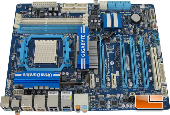
As I mentioned on the first page, aesthetics always take a back seat to features and performance. The GIGABYTE 890FXA-UD5 clearly has plenty of features for most, if not all users. As for performance, we will get to that shortly. First we should take a look at the layout of the GIGABYTE 890FXA-UD5 and see what makes it tick.
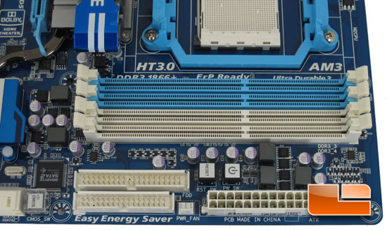
Starting out at the DIMM slots we can see that this corner of the board is packed with features. The DIMM slots will support four sticks of memory at 2000MHz (oc). Just below the memory we have the onboard power and reset switches. Below the switches we have the 24pin power and to the left of that we have a 3-pin fan header and the floppy and IDE headers.
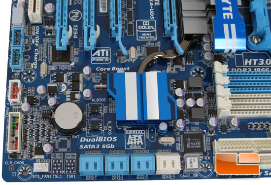
Sliding down the GIGABYTE 890FXA-UD5 we can see the clear CMOS button next to the mounting hole. Next to that we have eight SATA ports. The two white ones are SATA2 ports controlled by the GIGABYTE SATA2 chip above the clear CMOS button. The six blue SATA ports are SATA3 which are controlled by the AMD SB850.
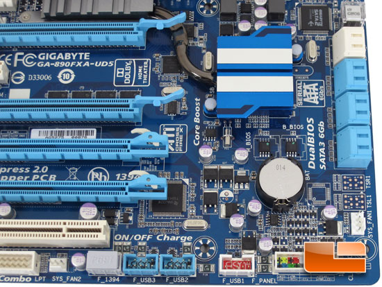
Spinning the GIGABYTE 890FXA-UD5 we can take a look at the front panel header (slightly behind the LR Logo). Here we can see three USB Headers, a Firewire header and a 3-pin fan header.
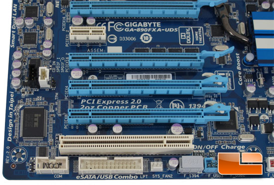
Next to the 3-pin fan header is the pin out for the parallel port and the com port.
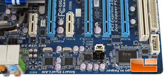
The large iTE chip on the right side of the photo is an IT8720f. To the left we have a cd in and the S/PDIF with the Realtek ALC889 codec. Just past the Realtek ALC889 codec is a pair of Realtek 8111D chips; these are the controller chips for the onboard nics that run at 10/100/1000 Mbits/s.
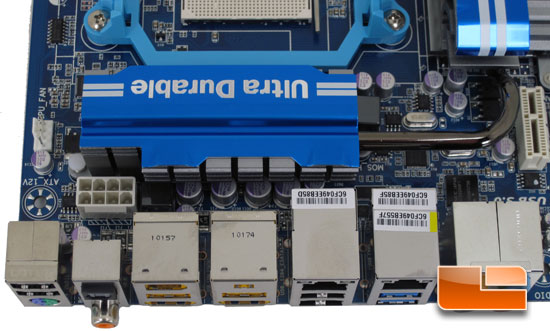
Behind the I/O panel we can see the solid capacitors on the GIGABYTE 890FXA-UD5 and the 8-pin CPU power, as well as the heat sink that keeps the 8+2 phase power circuitry cool. On the right side of the photo you can see the NEC USB3.0 chip.

You will find no shortage of parts on the I/O panel. There is a total of ten USB ports; the two blue USB ports are USB3.0 which are controlled by the NEC chip mentioned above. There is also a pair of e-SATA/USB2.0 combination ports. As for the remaining ports, there is a combination mouse and keyboard P/S2 port, an optical and coaxial S/PDIF out, a pair of IEEE 1394a (firewire) ports, a pair of gigabit onboard RJ-45 ports and six audio jacks.

Comments are closed.