ECS Factory Tour 2007 – Making a Motherboard
Solder Masking
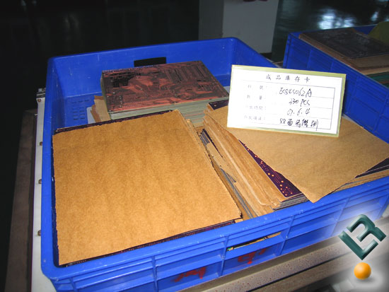
The boards are looking super clean after the cleaning process, but they still need to be cut.
Nothing like getting a little trim cut!
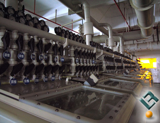
The boards are given one last wash to make sure they are spotless as they are about to have some color added to them. The machine that washes the boards is impressive. Check out all the valves and pressure gauges on that thing!
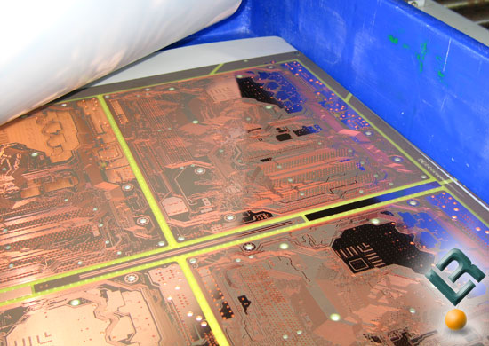
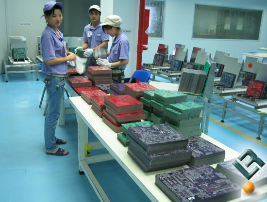
Once the boards are all washed they are broken down into the group they belong to, so they can head over to the solder mask printing area to get whatever color they need.
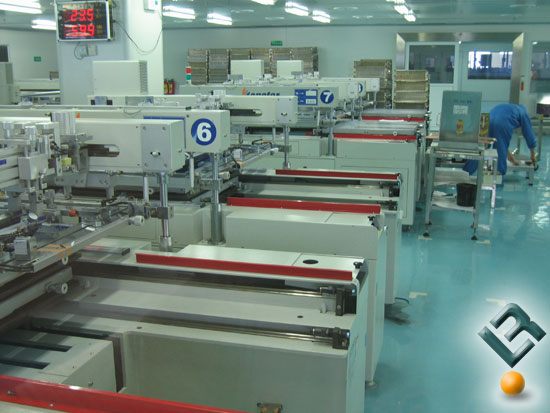
After the board is cleaned one last time the PCBs are cut and sent to the solder mask printing area, which is where a coating will be applied to the printed circuit board. This coating is designed to insulate and protect the copper traces and keep them from shorting together during the wave soldering process that takes place later when surface mounted components are installed.
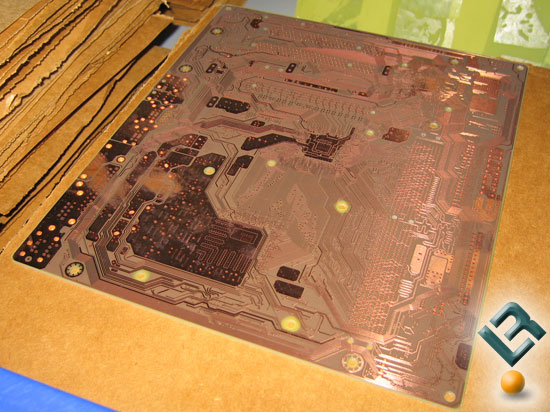
After the boards have cured all the logos, branding, model numbers and information about the boards’ features should be already printed on the PCB. The boards are now ready for the surface mount assembly line as the making of the PCB is finally completed!
Comments are closed.