AMD Reveals Polaris GPU Architecture – GCN 4.0
AMD’s Polaris Architecture was almost kept quite before CES 2016, but now AMDs Radeon Technologies Group has lifted the embargo holding back some of the first details of its new Polaris architecture for 2016 Radeon GPUs. AMD will be previewing the new GPUs that are said to offer solid gaming experiences at 61 percent less power than competing GPUs thanks to being built on the 14-16nm FinFET process.
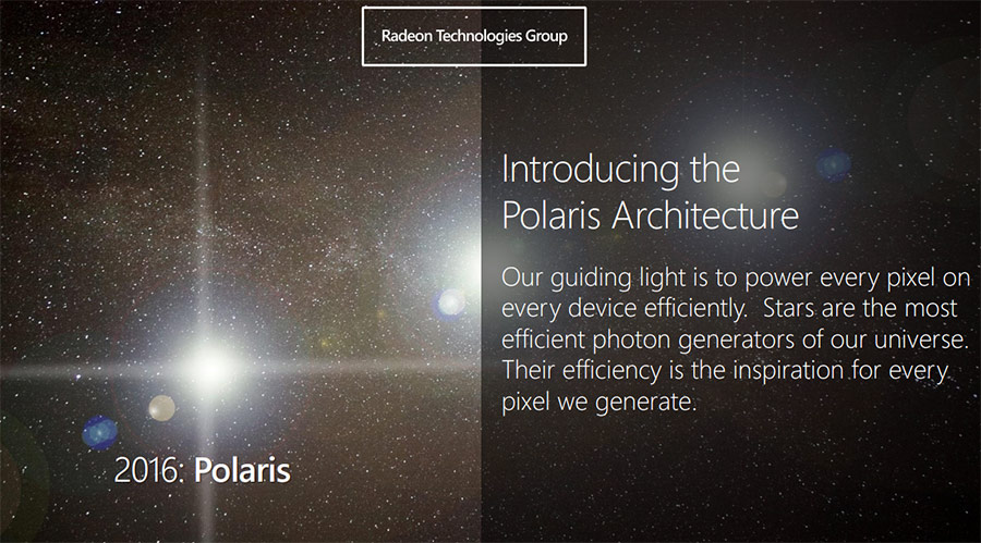
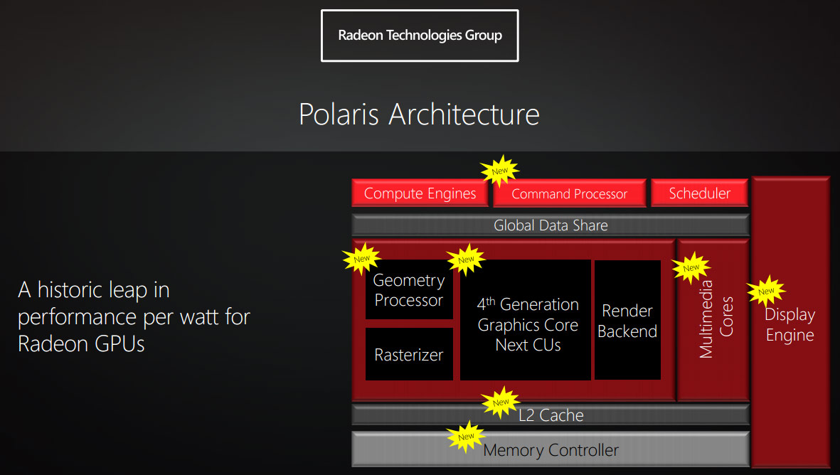
AMD did more than just shrink and change the manufacturing process as Polaris is a vastly redesigned GPU featuring 4th Generation GCN cores (GCN 4.0), a new memory controller, new multimedia cores, and a new geometry processor. AMD is calling Polaris an historic leap in performance per watt efficiency and it will open the door to unprecedented gaming and multimedia experiences in thin and light notebooks and desktop gaming PCs. Polaris is also known as the North Star, which famous for holding nearly still in the sky while the entire northern sky moves around it. Mariners relied upon to navigate the world for centuries and now AMD will be relying on it to stay competitive against AMD in the GPU market.
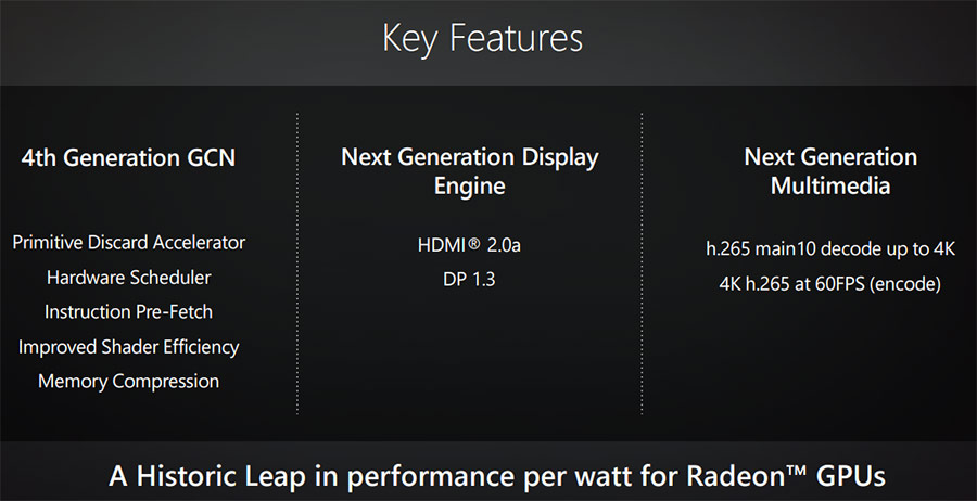
Many of our readers will be excited to learn that AMDs 4th generation Graphics Core Next architecture, a next-generation display engine offers support for HDMI 2.0a and DisplayPort 1.3. This is a pretty big deal and next-generation multimedia features enabling 4K h.265 encoding and decoding. High Bandwidth Memory (HBM) progression will continue, but right now GDDR5 is being used on the first Polaris GPUs. That leads us to believe that AMD will be rolling out Polaris on the mainstream graphics solutions first.
4th Generation GCN
- HDMI 2.0a
- DP 1.3
- 265 main10 decode up to 4K
- 4K h.265 at 60FPS encode/decode
- Largest performance per watt jump in the history of AMD GPUs
In a demo that Legit Reviews personally witnessed in person, AMD showed off a PC with an early Polaris GPU running Star Wars Battlefield that looked great. The Star Wars: Battlefront demo was shown on an Intel Z97 platform powered by an Intel Core i7-4790K with 8GB (2x4GB) DDR3 1600MHz of memory running Windows 10 64-bit with a screen resolution of 1920×1080. The performance of that system with the Polaris GPU was 60 FPS with a total system power draw of 86-88 Watts of power on average. The exact same system outfitted with an NVIDIA GeForce GTX 950 consumed 143-150 at the same performance level, so AMD had over a 2x perf per watt advantage against this specific competing GPU. You can see AMD do that demo again in the video clip above
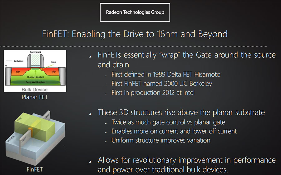
Transistors per area are still doubling effectively every two years but leakage was getting worse at the same rate. To reduce leakage, AMD is using multiple voltage islands, back bias or advanced circuits for clock gating to help reduce leakage in idle/sleep states. FinFET helps increase the transistor area and reduce the leakage while at the same time allowing you to enable and disable gates quicker/harder and that is key. The amount of power a transistor can handle dedicates the height of the fin. AMD is making all the fins the same height and that uniformity helps AMD keep power efficiency up. FinFET transistors have a 30-35% performance advantage over 28A planar transistors.
The first GPUs based on the Polaris architecture will ship in mid-2016 and it will be first available for laptops. That will be right around the same time we expect NVIDIAs next GPU architecture called Pascal to debut and it just happens to be using the 16nm FinFET process by TSMC. Most gamers are hoping that AMD will be able to a great graphics card as they don’t want NVIDIA to have a Monopoly and be able to control video card pricing.