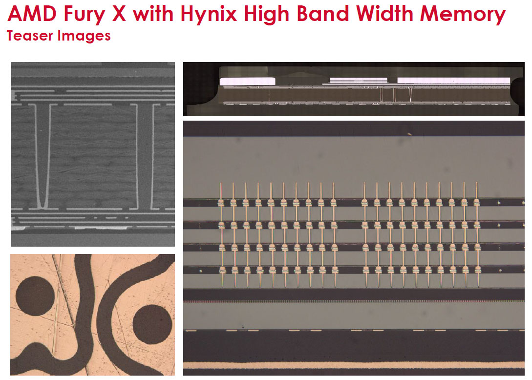
AMD Radeon R9 Fury X Fiji’s GPU Seen Like Never Before
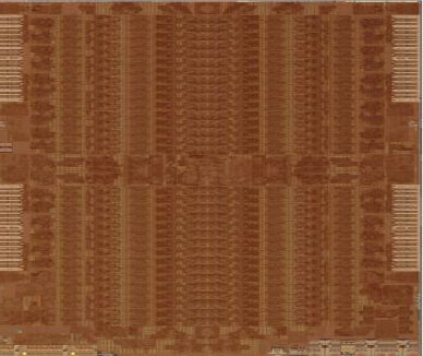
Chipworks is working on creating a package analysis report detailing the Fiji GPU with Hynix’s High Bandwidth Memory (HBM) that is used by AMD’s Radeon R9 Fury X desktop graphics card. Reports like this usually cost a small fortune, but at least we can look at the teaser shots and see some of the inner workings that we’d normally never see as PC enthusiasts and gamers. This is our first real look at AMD’s new silicon interposer that made its debut on the AMD Fiji GPU earlier this year.
We ran across this news on 3DCenter.org and they die shots show where the four HBM stacks are located on the GPU. Note the size of one of the four 1024-bit HMB segment versus that of the one of the six 64-bit GDDDR5 bus segments on Tonga that make up that GPUs 384-bit memory interface! It’s much smaller than we expected!
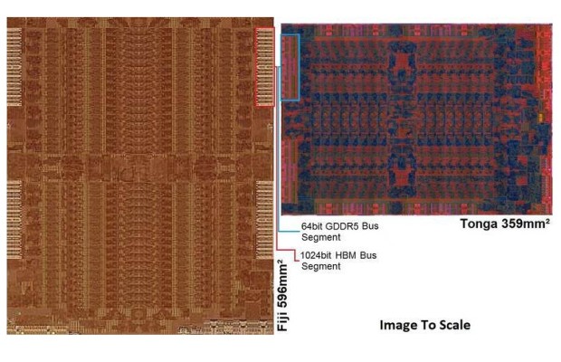
Keep in mind that HBM takes up 50% less PCB space, uses less power and has much higher performance and we can quickly see why AMD and NVIDIA are moving to HBM technology.